EAGLE is an electronic design automation (EDA) software that most printed circuit board (PCB) designers like to use to connect schematic diagrams, component placement, PCB routing, and comprehensive library content.

Like the initial design files from Altium, PCB manufacturer can not directly use these initial files from Eagle for computer aided manufacturing due to different software platform. The circuit board designer need to convert it as Gerber files before sending them out a for a PCB quotation or fabrication purpose.
How To Create PCB Gerber Files from Eagle Files
In this Gerber tutorial, we will introduce how to create the files you need for a 2-layer board using Cadsoft Eagle. After you have completed this tutorial you will have all the necessary files needed to send to us for your PCB manufacturing or a quotation.
Step 1: Open the CAM Processor

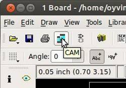
In the Eagle, open Board view. Click the “CAM” button or choose “File->CAM Processor”. This will open the CAM Processor tool that is used to generate the files.
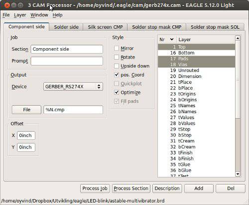
Here you can define the sections you want to create files for.
But you don’t really need to understand this. Actually we have never really thought about the details of this until we were writing this article. We have just been using ready-made configurations. And that is probably what you want to do as well.
Step 2: Open a predefined job
To simplify creating Gerber files, Eagle comes with a predefined job for this. It is called gerb274x.cam.
To open it in the CAM Processor click “File->Open->Job…”
Browse to your …/eagle/cam/ folder, and you should see a file called gerb274x.cam. Choose it and click “Open”.
You will now see five tabs in the CAM Processor. Each of these tabs will generate a Gerber file.

Step 3: Adding a Second Silk Screen (Optional)
If you look at the tabs, you will see that you don’t have a file for silkscreen bottom. For simple boards, the silkscreen is usually on the top layer so that you don’t need the bottom. Some of the cheap circuit board manufacturers don’t even allow bottom silkscreen,but we are OK that you design Both top and bottom silkscreen layers.
So, if you need silkscreen on bottom layer as well, follow these steps:
Click “Add”
Change Section to something like “Silk Screen SOL”
Change File to “%N.pls”
Deselect all layers
Select layers 20 “Dimension”, 22 “bPlace” and 26 “bNames”
There you go.
Step 4: Create Each Gerber File
Select where you want to put the Gerber files by clicking on the “File” button and choosing a folder. Do this for all the tabs.
Then click “Process Job”. This creates your Gerber files.
Step 5: Adding File for Drill Holes
Even though drilling is supported by the Gerber format, manufacturers usually want the Excellon file format for specifying drill holes. Luckily, Eagle also comes with a predefined job for creating a drill file.
Open it in the CAM Processor by clicking “File->Open->Job…”
Browse to your …/eagle/cam/ folder, and open the file named “excellon.cam”.
Select where to put the output file by clicking on the “File” button.
Then click “Process Job” to create your Excellon file.
Step 6: Check Output Files

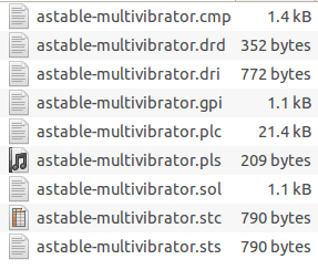
You should now have the following files:
| *.cmp (Copper, component side) *.drd (Drill file) *.dri (Drill Station Info File) – Usually not needed *.gpi (Photoplotter Info File) – Usually not needed *.plc (Silk screen, component side) *.pls (Silk screen, solder side) *.sol (Copper, solder side) *.stc (Solder stop mask, component side) *.sts (Solder stop mask, solder side) |
After you have created each gerber file, you should always look at them using a Gerber viewer (Such as CAM350-download ) to make sure everything is ok.
Summary
This Gerber tutorial shows one way of creating the files you need. Even though this should be OK for many PCB manufacturers, you might find that some would want the files created in a slightly different way. If so, don’t worry, we will probably provide you with a job file you can load directly into Eagle or at least have a good explanation on how to do it on our website.


