Generally, the NPI (new product introduction) process is complex. A new product probably consist of hundreds to thousands of new parts, each of which may involve unique design, specifications, development and other specialized requirements.
WELLER’s experience let us know that a successful new product introduction determined by some key factors such as integration of the product design and the design processes align seamlessly with your product launch and manufacturing strategy. Our NPI process helps clients launch complex products by providing extensive manufacturing, testing and engineering expertise.
At WELLER, we absolutely ensure our clients get a quick turn on their PCB fabrication and assembly services and provide both scalability for volume manufacturing, as well as the flexibility to respond to your needs-meeting your quality, delivery and price requirements.
Contact us for more information about our NPI services to help you quickly launch your next product to the market.
Complete End-to-End NPI Services
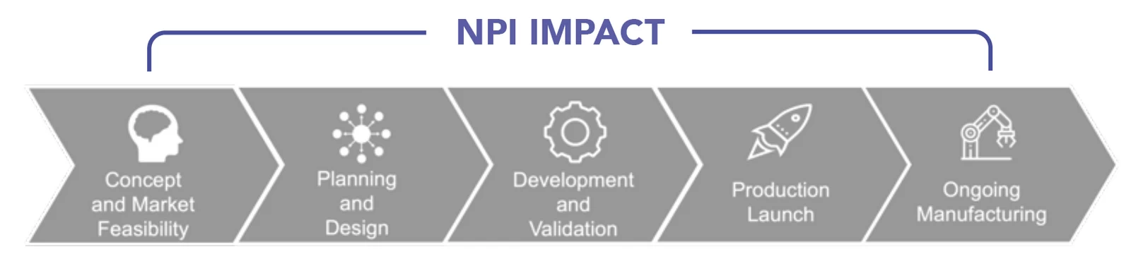
Proven NPI & Transfer Process
When you cooperate with WELLER, you will get the benefits of our experience with launching new products through our learned best practices, knowledgeable resources and abundant Technology Accumulation. WELLER’S proven NPI process helps original electronics manufacturers launch complex products by providing quality manufacturing, technical support and superior engineering services, as well as flexible NPI program management methods and logistics assistance.
Seamless Prototype To Volume Solutions
WELLER provide full-solution in electronics manufacturing, rapid prototyping service to our global customers. WELLER adds competitive value to customers by providing complete prototyping, design support, value engineering consult services (DFx), build and testing services all offered under WELLER, resulting in unmatched speed-to market support with reduced go-to-market risk.
Advanced Manufacturing Solutions
Our team have over 20 years of experience building highly complex assemblies…at high quality! Experience gained from cooperating with some world class EMS customer allow us to manage your project according to ISO standards. dynamically providing the necessary feedback to your engineers that will validate, reduce cost and simplify future production of your design.
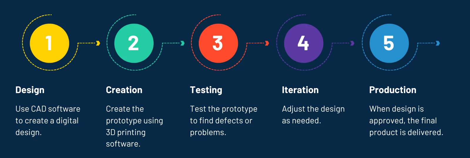
Our Prototype Assembly Process Provides:
Advanced Rapid Prototyping Process
Our Standard Lead Time
Offerings
WELLER Benefits
Building Products For Success
Design Services – Prototyping Support
If you need any assistance regarding design schematics, WELLER can provide necessary support behind your this critical first step. Our expert consulting design engineers (available based on your project’s requirements) can collaborate with your designs to create schematics and PCB layouts (by software Altium or Cadance, including Gerber files and BOM) to your specifications -incorporating DFM/DFA/DFT principles throughout the process.
Engineering Services – Value Engineering (DFX) & Feedback
With over 20+ years of electronic manufacturing experience, our team is acutely aware of the impact a well-designed PCB assembly can have on the near and long-term costs associated with the manufacturing and testing of your PCBA, as well as your final product’s speed to market. Our design for excellence (DFx) review process provides DFSC/DFF/DFA/DFT/DFM improvement recommendations to your engineering team throughout the entire “concept to completion” process.