Printed Circuit Board Assembly X-Ray Inspection
WellerPCB has been striving for providing high-quality PCB manufacturing and PCB assembly for clients from all over the world at competitive prices since our establishment. Due to the development of Surface Mount Technology and increasing complexities of electronic products, high-density and small PCBs account for the majority. As a main form of structural test and inspection, Automated Optical Inspection is only applicable for defects that are relatively easier found such as open circuits, solder bridges, solder shorts, insufficient solder and excess solder. However, because pins of BGAs are hidden under the chip package, it’s difficult to test them only based on light. That’s why Automated X-Ray Inspection (AXI) is required.
Belonging to the same structural test and inspection category, AXI shares the same principle with AOI, that is, inspection is carried out through capturing images. The difference between them lies in the source in that AOI depends on light source to capture images while AXI on X-Ray. Materials absorb X Rays according to their atomic weight proportion. Materials made of heavy elements get more X Rays absorbed while those made of light elements get fewer. As a result, materials absorbing more X Rays are displayed more obvious or darker in their images than those absorbing fewer Rays. When it comes to PCBA, solder joints are made of materials with heavy elements while other parts such as most packages, silicon ICs and component leads are made of materials with light elements. Therefore, high-quality solder joints should look darker or more obvious on images than other parts.
Based on its working principles and capabilities, AXI is applied to test circuit boards containing components with array-style packaging or fine pitch packaging including BGAs, CGAs (Column Grid Arrays), CSPs (Chip Size Package), etc. AXI is usually placed in the assembly process, just after the last soldering no matter wave soldering or reflow soldering. Furthermore, AXI is usually applied coupled with boundary scan test, ICT and functional test in order to obtain optimal inspection results.

AXI features: some advantages as a type of structural test and inspection
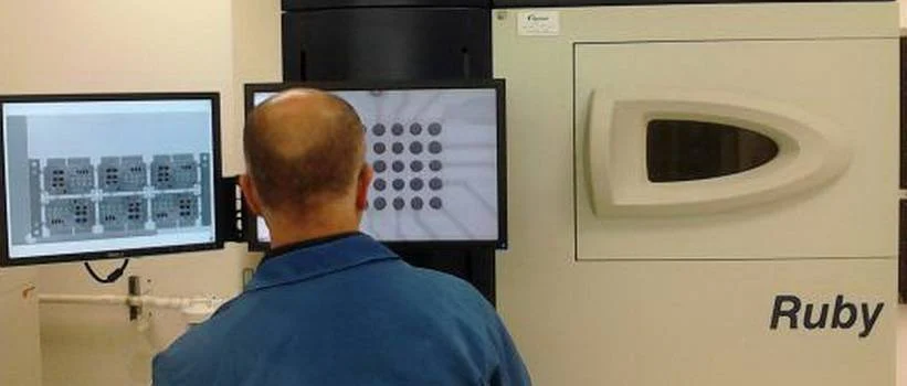
AXI equipment is classified into two categories: 2D and 3D equipment. For 2D AXI equipment, WellPCB uses model VIEWX2000, responsible for inspecting PCBA manufacturing defects including opens, shorts, insufficient solder, excessive solder, missing electrical parts, misaligned components, solder voiding etc.
Although AXI and AOI have the same working principles and play similar roles in PCB assembly production line, defects they can detect differ to some extent.
Inspection capability comparison between AXI and AOI
| Defect Type | AOI | AXI | ICT |
| Faulty component | × | √ | √ |
| Missing component | √ | √ | √ |
| Incorrect component value | × | × | √ |
| Lifted Lead | √ | √ | √ |
| Misaligned/Misplaced component | √ | √ | √ |
| Open Soldering Circuits | √ | √ | √ |
| Solder bridges | √ | √ | √ |
| Solder shorts | √ | √ | √ |
| Insufficient solder | √(not heel of joint) | √ | × |
| Solder void | × | √ | × |
| Excess solder | √ | √ | × |
| Solder quality | × | √ | × |
| BGA and CSP shorts | × | √ | √ |
| BAG and CSP open circuit connections | × | √ | √ |
Automated X-ray inspection is a critical quality control procedure of many electronics manufacturing organizations. X-ray inspection can provide a fast and accurate and thorough inspection of internal soldering quality passing the production facility and by this way provide real-time feedback that have the production system to be optimized to produce high quality and reliable electronics assembly. Generally, the cost of AXI is more expensive than some other forms of inspection, but it has many advantages and these need to be carefully balanced against the costs to ensure whatever choices is made, it is reasonably correct for the particular production and manufacturing environment.