After completing the research and development of a new electronic product design and getting prototypes from the electronic contract manufacturer, your primary work is to conduct comprehensive testing of the software and hardware, thoroughly inspect the functionality of the samples to determine whether they are functioning properly and introduce them into mid to high volume trial production.
Key Preliminary Inspections Before A Software Loading
If you are quite confident in your PCB schematic diagram design, the rest of the work can be attributed to the electronic manufacturing process. PCB fabrication and printed circuit board assembly are relatively complicated process, problems commonly come out from multiple factors such as open-short circuit, soldering joint short, cool soldering, fake components, wrong base material used in PCB fabrication, soldering opening in components, etc. Before loading software and firmware into your PCBA, below crucial inspections is worth to do:
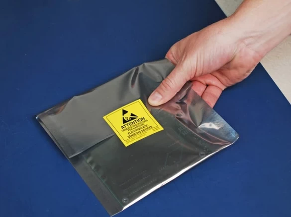
Packing Inspection:
Packing method is first impression and direct reflection on the professionalism of a contract manufacturer. Usually, the packing method can directly reflect whether a contract manufacturer is professional and reliable.
Firstly, the packaging materials should be environmentally friendly, and secondly, the materials of bags that packing PCBA be anti-static. If the printed circuit board assemblies you received at a poor of packing method: no anti-static bags protection, just bubble bags, with fragile box, no doubt you will question to the quality of the product.
Anti-static protective packaging is a basic condition for the transportation and storage of semi-finished electronic products can prevent potential electrostatic damage to the product and increase shelf-life.
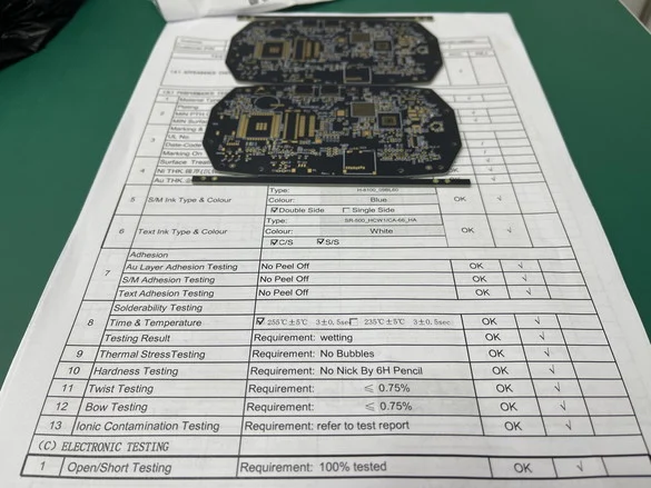
Outgoing Document Check List:
Commonly, a professional electronic manufacturer always attach a complete set of inspection and testing reports in paper along with the shipping goods. The content of this report presents the specifications requested by the customer and the final manufacturing results. For example, the type of the base laminate material, final PCB thickness, copper thickness, surface finishing ant its thickness, solder mask color, silkscreen color, the specific brand of the material, impedance testing report, etc. If the report fully lists the items as you requested and the actual manufacturing results as it is, it means your product exactly manufactured per your specific requirement. Or else, may be the supplier not exactly implements your requirement of manufacturing specification, and the submitted products should hide some potential quality problems and should catch file someday when you use it. This type of supplier often offer very cheap price, but you need to stay away from them to avoid any trouble.
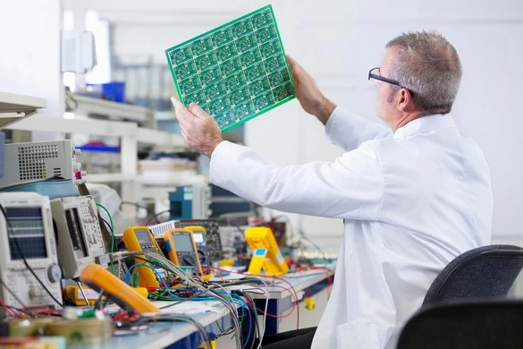
Cosmetic inspection:
A product with perfect cosmetic is the evidence of a manufacturer’s manufacturing capability and quality standard, and it is the in-direct reflection of the reliability.
Usually, a good PCB assembly manufacturer places high attention on the cosmetic issues of their manufactured product, and at least they will use IPC class 2 or higher standards as inspection criteria before releasing shipping, including defects or flaws such as, solder flux residue, slightly scrapes, and components soldering deviation, etc.
Anyway, the PCB assemblies with these defects or flaws can be shipped out only when they are proved and allowed by IPC documents that do not affect the reliability of the product.
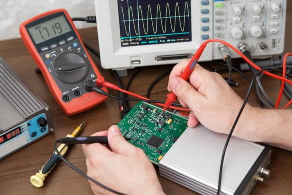
Electrical Path Testing:
If the incoming cosmetic inspection proved the PCB manufactured and assembled at good manner, next step is to power up the assembled printed circuit board by required voltage and test electrical path is good or not. This is a basic condition to confirm that there is no open or short circuit issues existing in the populated circuit board. The power normally loaded through some USB connectors or male header pins. This is subject to the PCB designer’s intention.
A desk power supply usually needed to do this work. Typically the input voltage is under 12V, and a multimeter is used to measure the output voltage on specific test points. This procedure can avoid the PCB or some crucial component smoked once direct high voltage load on a defect electrical path circuit board. Once all the output voltage run as expected, it can be proved that no electrical path flaws existing on the PCBA and can go to program software and inject firmware.

Software Setup And Firmware Injection
If the cosmetic inspection and power up testing proved good, next step is ready to load the software and perform firmware injection process. Typically this step is a common work only differ from various brand of chips.
Software Setup: Normally this is to setup the programmer software into a computer, such as ST Micro Installer and Driver, the firmware can only be injected through this tool software. The computer operated by windows system of Linux system, depending on the software environment of the PCBA.
Firmware Injection: Once necessary tool software installed, the next procedure is to inject the firmware into the MCU on the PCBA, the firmware is a unique code that design and programmed by the software engineer of the electronic circuit board.
Testing, Debug, And Repair.
Testing: This is to perform the full loop testing process including software and hardware, to check whether the core components acts as it is expected, such as humidity sensor, pressure sensor, etc. Generally, a set of checking list could be recorded from testing results.
Debug: “Nothing great comes into be all at once”. Multiple issues always come out at prototypes testing process: software version, program upgrading, compatible issues, etc. Usually it needs a back and forth work before a final success. Experienced software engineer would be time saved in this procedure.
Repair: The hardware flaws or defects usually detected out when proceed firmware running, some unexpected value need to be corrected via hardware optimizing, such as using resistors with narrow tolerance, large volume of capacitors, higher sensitivity instructor, more acute impedance, electrical path optimizing, and so on. A professional hardware engineer is needed in this process.
What Weller Can Offer?
As an experienced EMS manufacturer, WELLER support testing and debugging for various filed of customers: Medical, industrial, IOT, defense, power supply, etc. Here we have professional hardware engineer familiar with testing and debugging for multiple brand of Chips, such as ST serial, IT serials, we are good at schematic analysis and troubleshoots. You will be right to choose us as your reliable electronic manufacturer.