Underfill Techniques

Underfill is a process of using an epoxy or adhesive material to fill gaps between a chip and its carrier or and a chip and the PCB substrate.

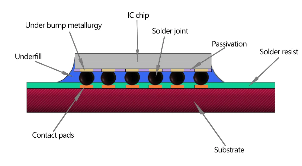
Underfill can properly protect the chips or semi-conductors from shock, drop, and vibration and helpfully reduces the strain on fragile soldering connections caused by the difference in thermal expansion between the silicon chip and its carrier (Two different materials).

It is a type of liquid polymer applied to the populated PCB (printed circuit board) after it has been subjected to the reflow process. Then it will be cured after placing the underfill. In this process the underfill encapsulates the bottom side of the silicon chip, filling the gap of the fragile interconnected pads between the chip’s bottom side and the PCB’s top side.

The primary purpose for considering the use of encapsulant underfill in electrical assembly is to reduce the impact of deviation in global thermal expansion characteristics between the silicon die and the underlying attached substrate. On conventional semi-conductors packaging, typically these stresses are absorbed by the natural flexibility of the wire leads. But, with direct-attach methods chips like solder ball arrays, the solder joints themselves dot represent the stress points in the structure and therefore are the most susceptible to stress failures. Unfortunately, these are also the most critical because a failure at any interconnect point would leads to the functionality failure of the circuit. By thoroughly filling into gaps between the chip, solder balls and PCB substrate, the underfill material can redistribute the strains and stresses from the coefficient of thermal expansion (CTE) mismatch and mechanical shock over the entire chip area.

2023/12/Underfill-Techniques.webp

Another benefits from underfilling is it’s production against moisture and other forms of contamination. But the negative factor raised up that the use of underfill increase the overall cost to the manufacturing operation and take difficult to rework. Therefore, most manufacturers perform a necessary functional test after reflow process and prior to the underfill operation.

When to Underfill

Because there are at least 50 different designs of CSP(chip scale package), plus a numbers of variables and operating conditions involved in interconnect design, it is difficult to provide a specific definition for when to use underfill. However, there are a myriad of key factors that should be taken into account when starting a PCB design. Including some of the critical factors:

Different CTE value between the die and the PCB substrate. Typical PCB material has a CTE of 16ppm; silicon of the die has a CTE of 2.4 ppm. Generally ceramic materials can be designed to have a matching CTE but 95% alumina ceramic has a CTE of 6.3 ppm. Although underfill proved much reliability on ceramic substrates, it has greater needs on PCB-based packages. An alternative solution is to use an interposer substrate as a shock absorber between the chip and the main substrate, such as flexible or high-CTE ceramic materials, which can reduce the impact that due to the CTE differences between PCB and silicon die.

The die size. Generally, the larger the die area take along with the greater strain-induced problems. For example, one study proved that once the die size increased from 6.4 to 9.5mm, the number of temperature cycles from -40° to 125°C that the interconnect could withstand decreased from 1,500 to 900 cycles.

The solder ball size. The solder ball size and layout of the chip play a critical role in the underfill evaluation because larger ball sizes, such as ball size in diameter with 300µ that are typically used with CSPs, these are more robust and can handle stress and strain much better than the 75u diameters balls used with flip chips. Assuming the relative sheer strain displacement of a two-member joint is similar in CSP and flip chip, then strain withstood by the CSP solder joint is approximately a quarter of that experienced by a flip chip. Therefore, the chips designer originally thought that the CSP solder ball structure itself could afford the mechanical strains associated with PCB substrate and die thermal expansion. A serial of studies have shown that underfill offers an excellent reliability benefit with CSPs, particularly in some portable applications. On the layout handling, some electronic designers have found that increasing the size of the lands at the chip corners can improve strain resistance, but this is not always a practical or sufficient option to achieve reliability goals.

 Integrated PCB thickness. Experiments have shown that thicker PCBs are stiffer and resist bending forces from impact shock more than thinner circuit boards. For example, some analysis has demonstrated that an increase of FR-4 substrate thickness from 0.6 to 1.6 mm could improve cycles-to-failure from 600 to 900 cycles. Unfortunately, the reality in many of today’s miniature electrical devices is that it is often limited to increase substrate thickness. In practice, each doubling of substrate thickness can provide approximately a 2 times of improvement in reliability, but a doubling of die size will impose a 4 times of degradation.

Application environment. In the final analysis, the decisive factor generally have to do with increasing expectations for survivability. For example about the the specifications on hand-held devices (cell phones, pagers, etc.), it is becoming common to call for normal functioning after thermal cycling between -40° to 125°C for 1,000 cycles and survivability after 20 to 30 drops from 1 m onto a concrete floor.

Some researches on thermal cycling show that using underfill can improve the number of -40°C to 125°C temperature cycles to be 2 to 4X. These temperature cycles that can be explored prior to exhibiting failure modes, with some assemblies handled with underfilling still not failing after as many as 2,000 cycles. When compared with the actual costs of field failures (e.g. returns, loss of reputation, etc.) for devices exposed to increasingly harsh environments, many manufacturers are actively considering to use underfill as a reliability insurance method.

When it comes to decide to use underfill technology to handle the chips package on electronics assembly, a range of challenges need to be taken into account to efficiently implement the process to achieve consistently reliable and durability results while maintaining required mass production throughput levels. Some of critical issues including:

Achieving complete and void-free flow under the die.

Dispensing around closely packed die.

Avoiding contamination and impact to other components.

Dispensing through openings in RF (radio frequency) shields or enclosures.

Controlling flux residues.

Contact WELLER Now with Your Flip-chip Underfill Needs