Weller has been in the printed circuit board design business since 2010. We specialize in high-speed PCB design, SI/PI/EMC analysis in addition to training and consulting. With our outstanding expertise at PCB design and printed circuit board layout, we offer high-quality service for over 2,000 clients all over the world. We are not the largest PCB design center in China but we have over 11 professional engineers that full skilled at PCB layout for communication projects.
PCB Layout Capability
| Max layout layer count | 56L |
| Max pin qty. | 150000+ |
| Max connect qty | 120+ |
| Min track width | 2.4mil |
| Min track spacing | 2.4mil |
| Impedance design | Yes |
| Min via hole size | 6mil(4mil for laser drilling) |
| Max BGA qty | 120+ |
| Min BGA pitch | 0.3mm |
| Max BGA pins | 8371 |
| High speed signals | 112G-PAM4 |
| Blind and buried holes design | Yes |
Experiecne and Team
The most projects we participate in: Communication Server, Communication Switch, Bitcoin Mining.
| Role | Qty | Skilled years |
| Team leader | 1 | 10+ |
| Senior engineer | 6 | 5+ |
| Primary engineer | 4 | 1+ |

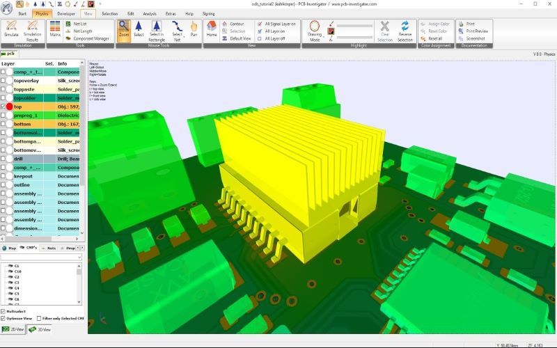
The CAD/Software We Use
Both Cadence Allegro and Altium Designer are common to our PCB designer engineer.
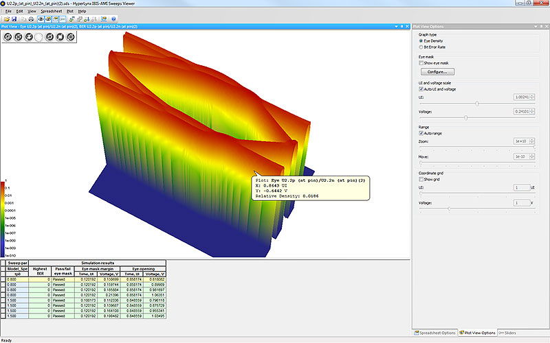
SI/PI/EMC Analysis
| DR3,DDR4 signal and Timing Analysis |
| High Speed Serial date analysis (25Gbps+ backplane) |
| PI analysis (PDN and IR Drop simulation) |
| EMC/EMI Design |
EMC Analysis
| System Level EMC |
| Board Level EMC |
| Chip Level EMC EMC Test |
| EMC Test |
Backplane PCB design, High-Speed PCB design, A/D PCB design, HDI/ALIVH/Buried resister/Buried capacitance, Flex PCB/Rigid-Flex Board, ATE. for the purpose of application in IT Communication, Computer, Medical, Digital and Consumer electronics.