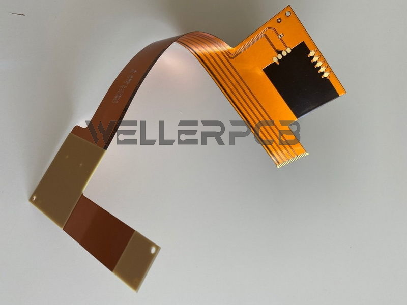
Different from rigid printed circuit boards, flexible circuit board (FPCB) is a special type of printed circuit board with it’s special property of bendable feature. The demand for flexible PCBs is increasing growing in electronic filed with especially strong demands from medical, defense and industrial markets.
Widely Application
As flexible printed circuit board can provide a great solution to connection between rigid PCBs with a reliable and repeatable electronic product. So, they have so many and wide applications that it would be impossible to completely list them all here.
Outstanding Advantages
Flex PCB provide a third dimension to connect between rigid PCB boards or to the interface between a printed circuit board and a remote electronic device. For example a sensor or a camera as in a mobile phone. They offer a light-weight solution to make the electronic product more and more lighter in weight, nearly half the weight of a rigid or a cable harness, to interconnections;as well much thinner in thickness.
Whats more, flexible PCB are also highly robust and can be flexed numerous times without any degradation to the electronic product. In a thorough designed dynamic situation, the flex PCB can go through millions of bendable cycles, a common existing example would be on an inkjet printer head. They also have the advantage of absorbing some unexpected shock so in a small device, such as a cell phone, they can take an impact without any damage to disconnect to the circuits.
They are also widely used to mount LEDs strips for applications such as down lighters on kitchen benches, outside deck lighting, etc. And, safety lights applied in transport systems, for example planes, trains and boats all utilise LED flex strip for guide sign of the emergency exit routes.
The Cost Alert of Printed Circuit Board
Normally, the cost of flex PCBA is more expensive than a standard rigid PCB assembly, but it can be optimized and saved by the optimized design and using it in the right application. Plus it’s lighter weight and less time in assembly process, coupled with the reliability which makes flexible printed circuit board a worthwhile consideration. It’s cost variations are mainly base and overlay thickness, typically 0.001” to 0.002”, different copper thickness, single or double sided plated through hole. Flex or rigid Stiffeners are an option which can help in handling during flex PCB assembly and allows electronic components to be assembled to the product easier. Another cost factors is from it’s raw material, big gap cost between famous raw material provider such as Panasonic and DuPont and normal base material manufacturer such as Taiflex.

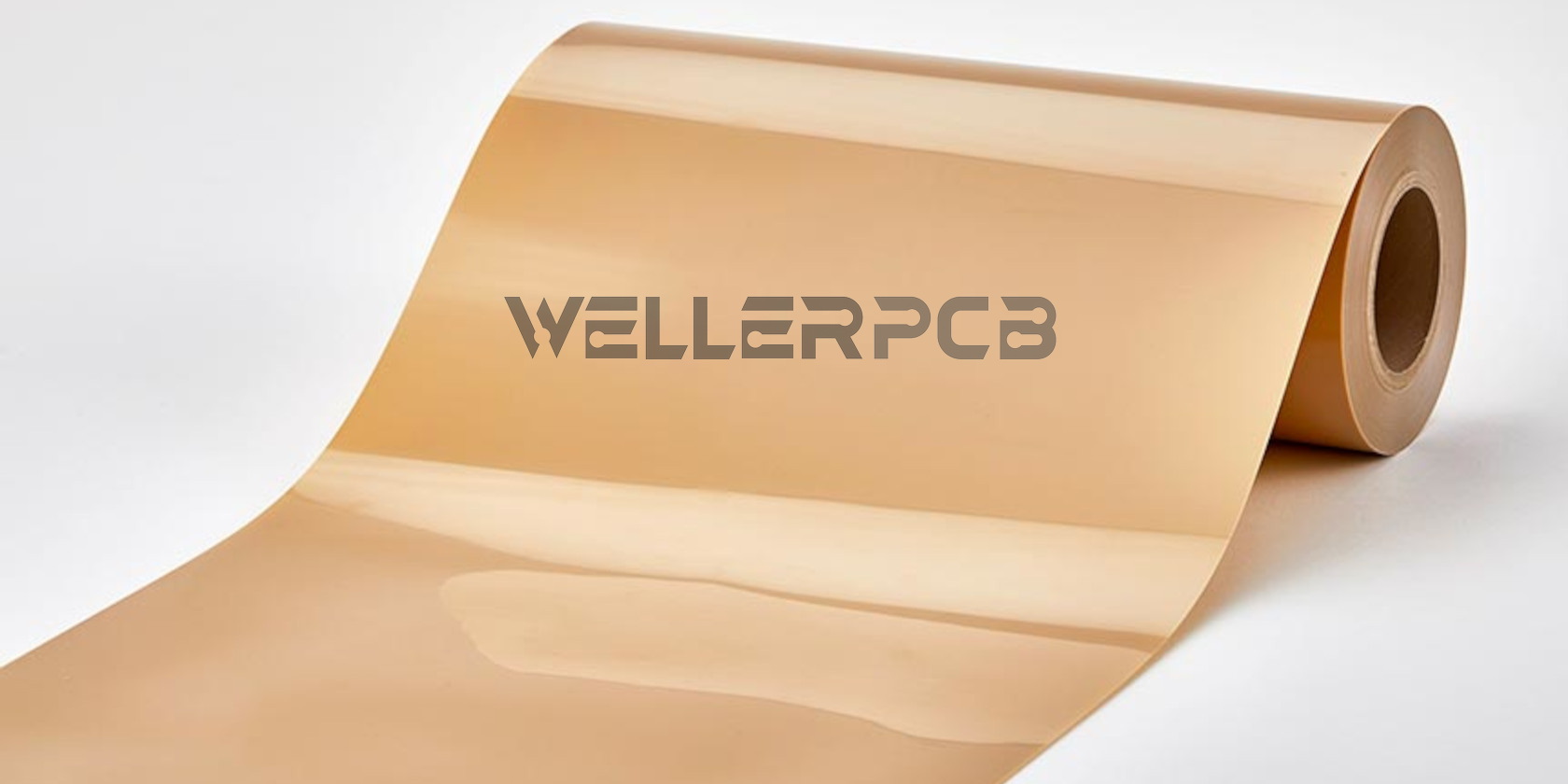
Flex PCB Base Materials
Weller Technology only uses hi-temp resistant Polymide (PI) materials unless customer insist to use low grade of material to cost down the price. Our preferred types are Panasonic and DuPont adhesiveness materials, and Shengyi adhesive-based materials and coverlayers.
Chosse Weller as your flex PCB manufacturer
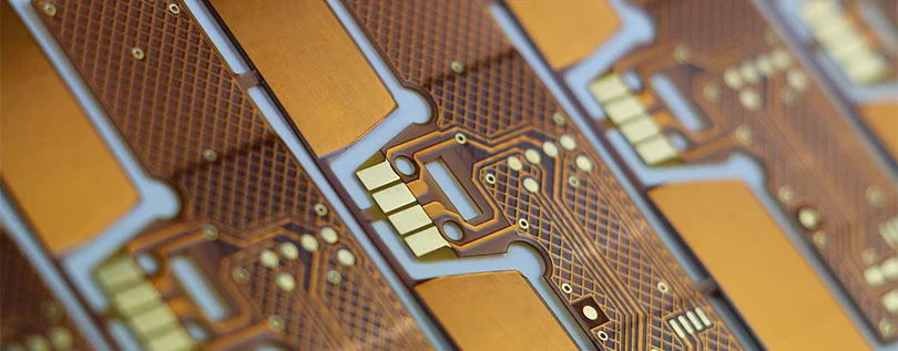
Weller Technology has the advanced capabilities to build types 1 through 4 flexible printed circuits. Most FPC’s are designed as single-sided or double-sided, as bend-ability is reduced with increasing copper layers and thickness. We have flex PCB manufacturing capability from single flex PCB to multi-layer flex PCB (up to 4 layers), as well Rigid-flex circuits.
Flexible PCB Manufacturing Capability
| Item | Product | Standard Flex Circuits | Standard Rigid-flex Circuits | High Density Interconnect (HDI) Flex Circuits |
| 01 | Standard Panel Size | 250mm x 400mm | 100mm x 100mm | 250mm x 400mm |
| 02 | Line Width and Spacing | .003″ (0.07mm) | .003″ (0.07mm) | .003″ (0.07mm) |
| 03 | Copper Thickness | >=1/2 oz | 1/4 to 1/2 oz. | >=1/2 oz |
| 04 | Layer Count | 10 | <=4 | <=8 |
| 05 | Minimum Drill (Mechanical) Hole Diameter | .008″ (0.2 mm) | .006″ (0.15 mm) | .008″ (0.2 mm) |
| 06 | Minimum Via (Laser) Size | 5.0mil (0.15 mm) | 1.0mil (0.025mm) | 6.0 mil (0.15 mm) |
| 07 | Minimum Micro Via (Laser) Size | 3.0 mil (0.07 mm) | 1.0 mil (0.025 mm) | 3.0 mil (0.07 mm) |
| 08 | Stiffener Material | Polyimide / FR4 / Metal | Polyimide / FR4 / Metal | Polyimide / FR4 |
| 09 | Shielding Material | Copper / Silver Ink / Tatsuta / Carbon | Copper / Silver Ink / Tatsuta / Carbon | Copper / Silver Ink / Tatsuta / Carbon |
| 10 | Via Tooling Tolerance | 2.0 mil (0.05 mm) | 1.0 mil (0.025 mm) | 2.0 mil (0.05 mm |
| 11 | Zif Tolerance | 2.0 mil (0.05 mm) | 1.0 mil (0.025 mm) | 2.0 mil (0.05 mm) |
| 12 | Solder Mask Bridge Between Dam | 5.0 mil (0.13 mm) | 4.0 mil (0.11 mm) | 5.0 mil (0.13 mm) |
| 13 | Solder Mask Registration Tolerance | 4.0 mil (0.11 mm) | 4.0 mil (0.11 mm) | 5.0 mil (0.13 mm) |
| 14 | Coverlay Registration | 8.0 mil (0.20 mm) | 5.0 mil (0.13 mm) | 8.0 mil (0.20 mm) |
| 15 | Coverlay PIC Registration | 7.0 mil (0.18 mm) | 4.0 mil (0.11 mm) | 7.0 mil (0.18 mm) |
| 16 | Coverlay Solder Mask Registration | 5.0 mil (0.13 mm) | 4.0 mil (0.11 mm) | 5.0 mil (0.13 mm) |
| 17 | PI Stiffener Registration | 10.0 mil (0.25 mm) | 10.0 mil (0.25 mm) | 10.0 mil (0.25 mm) |
| 18 | PI Stiffener Thickness Tolerance | 10% | 10% | 10% |
| 19 | FR4 Stiffener Registration | 10.0 mil (0.25 mm) | 10.0 mil (0.25 mm) | 10.0 mil (0.25 mm) |
| 20 | FR4 Thickness Registration | 10% | 10% | 10% |
| 21 | Legend Minimum Height | 35.0 mil (0.89 mm) | 25.0 mil (0.64 mm) | 35.0 mil (0.89 mm) |
| 22 | Legend Minimum Width | 8.0 mil (0.20 mm) | 6.0 mil (0.15 mm) | 8.0 mil (0.20 mm) |
| 23 | Legend Minimum Space | 8.0 mil (0.20 mm) | 6.0 mil (0.15 mm) | 8.0 mil (0.20 mm) |
| 24 | Legend Registration | +/- 5 mil (0.13 mm) | +/- 5 mil (0.13 mm) | +/- 5 mil (0.13 mm) |
| 25 | Legend Impedance | +/- 10% | +/- 10% | +/- 10% |
| 26 | Steel Rule Die Outline Tolerance | 5.0 mil (0.13 mm) | 2.0 mil (0.051 mm) | 5 mil (0.13 mm) |
| 27 | Steel Rule Die Minimum Radius | 5.0 mil (0.13 mm) | 4.0 mil (0.11 mm) | 5.0 mil (0.13 mm) |
| 28 | Steel Rule Die Inside Radius | 20.0 mil (0.51 mm) | 10.0 mil (0.25 mm) | 31.0 mil (0.79 mm) |
| 29 | Steel Rule Die Punch Minimum Hole Size | 40.0 mil (1.02 mm) | 31.5 mil (0.80 mm) | N/A |
| 30 | Steel Rule Die Tolerance of Punch Hole Size | +/- 2 mil (0.051 mm) | +/- 1 mil (0.025 mm) | 31 mil (0.79 mm) |
| 31 | Steel Rule Die Slot Width | 20.0 mil (0.51 mm) | 15.0 mil (0.38 mm) | 31.0 mil (0.79 mm) |
| 32 | Steel Rule Die Tolerance of Hole to Outline | +/-3 mil (0.07 mm) | +/- 2 mil (0.051 mm) | +/- 4 mil (0.11 mm) |
| 33 | Steel Rule Die Tolerance of Hole Edge to Outline | +/- 4 mil (0.11 mm) | +/- 3 mil (0.07 mm) | +/- 5 mil (0.13 mm) |
| 34 | Steel Rule Die Minimum of Trace to Outline | 8.0 mil (0.20 mm) | 5.0 mil (0.13 mm) | 10.0 mil (0.25 mm) |
Contact us freely if you have some questions on flex PCB design or you have a flex printed circuit board which needs to be manufactured at high quality standard with great grade of materials.