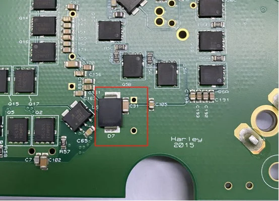
We focus on the field of pcb more than 20+ years,and we have ISO9001 quality management system certification,
rosh,ISO14001 environmental management system certification,TS16949 automobile quality management system certification and other certification.
| Item | Rigid PCB |
| Max Layer | 60L |
| Inner Layer Min Trace/Space | 3/3mil |
| Out Layer Min Trace/Space | 3/3mil |
| Inner Layer Max Copper | 6oz |
| Out Layer Max Copper | 6oz |
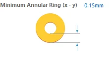
| Min Mechanical Drilling | 0.15mm |
| Min Laser Drilling | 0.1mm |
| Aspect Ratio(Mechanical Drilling) | 20:1 |
| Aspect Ratio(Laser Drilling) | 1:1 |
| Press Fit Hole Ttolerance | ±0.05mm |
| PTH Tolerance | ±0.075mm |
| NPTH Tolerance | ±0.05mm |
| Countersink Tolerance | ±0.15mm |
| Board Thickness | 0.4-8mm |
| Board Thickness Tolerance(<1.0mm) | ±0.1mm |
| Board Thickness Tolerance(≥1.0mm) | ±10% |
| Impedance Tolerance | Single-Ended:±5Ω(≤50Ω),±7%(>50Ω) |
| Differential:±5Ω(≤50Ω),±7%(>50Ω) | |
| Min Board Size | 10*10mm |
| Max Board Size | 22.5*30inch |
| Contour Tolerance | ±0.1mm |
| Min BGA | 7mil |
| Min SMT | 7*10mil |
| Surface Treatment | ENIG,Gold Finger,Immersion Silver,Immersion Tin,HASL(LF),OSP,ENEPIG,Flash Gold;Hard gold plating |
| Solder Mask | Green,Black,Blue,Red,Matt Green |
| Min Solder Mask Clearance | 1.5mil |
| Min Solder Mask Dam | 3mil |
| Legend | White,Black,Red,Yellow |
| Min Legend Width/Height | 4/23mil |
| Strain Fillet Width | / |
| Bow & Twist | 0.3% |


