DFM Check
It would be very excited when you finish developing and designing a new printed circuit board. But it is only the half of success as the next crucial step (DFM) is that the design must be facility to be manufacturing. It will get you result in high cost and poor production yield once your design is very “complex” and “high density”.

What is the DFM Analysis in Printed Circuit Board?
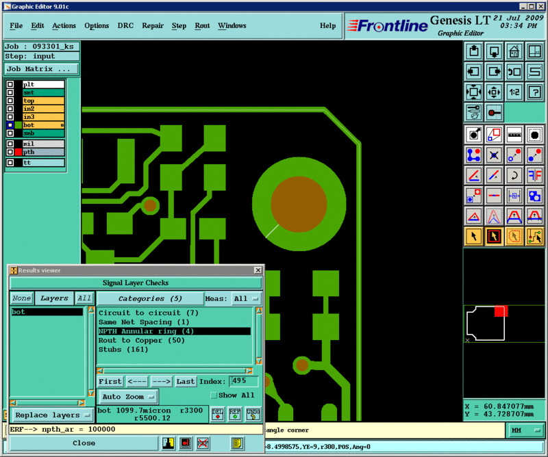
DFM is to input the design files into necessary software platform to perform a series of engineering analysis to determine the manufacturing viability of a PCB design along with specification and highlighting any manufacturing issues that may be visible from the design before formal production is carried out. This regular check allows a printed circuit board manufacturer to confirm whether the design is within the manufacturing capability.


What Can Weller Do for a DFM?
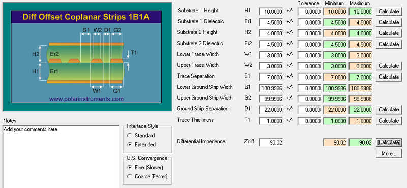
Weller is always your ideal partner when you develop a new PCB for your electronic product. No matter how difficult or how advanced it is, Weller can support you with timely response to make your time saved. The checking list including: laminate material, copper thickness, board thickness, surface finishing, track width/spacing, via holes density, spacing between holes and track, tolerances, matched trace impedance, etc.

What Result Weller Can Result in?
Here we have a professional team with experienced engineering and manufacturing knowledge from the service to some world class customers to provide DFM service (in printed circuit board manufacturing and PCB assembly) to your new product design.
| 1. To ensure the design can be the streamlinly manfuacturered. 2. Time saved. 3. Cost saved. 4. Can make a prototype based on your PCB design and provide sparring and guidance. |

