How to Choose Surface Treatment Process for PCB between HASL, Gold plating and Immersion gold
The choice of PCB surface treatment process depends mainly on the type of component that is finally assembled. And the PCB surface treatment process will affect the production, assembly and end use of the populated boards.
Surface Treatment Purpose
The most basic purpose of surface treatment is to ensure good solder-ability or electrical properties. Since copper in nature tends to exist in the form of oxides in the air, it is unlikely to remain as raw copper for a long time, so other treatments of copper are required. Although in the subsequent assembly, strong flux can be used to remove most of the copper oxide, the strong flux itself is not easy to remove, so the industry generally does not use strong flux.
Difference between Immersion Gold and Gold Plating on PCB Fabrication
Immersion gold and gold plating are often used in PCB fabrication process. Many PCB designers are unable to distinguish the difference between the two process. Some electronics designers even believe that there is no difference between them. This is wrong and must be corrected in time. So what kind of impact will these two processes have on the PCB? Let us explain it to you in detail, and help all of our customers to make the concept clear.
1. What is gold plating and immersion gold?
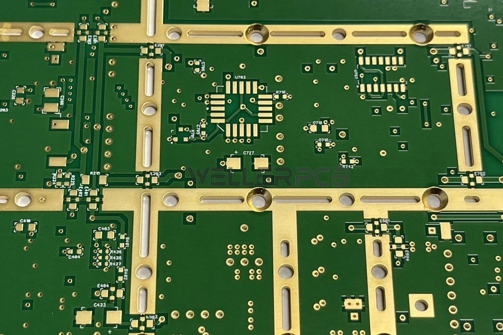
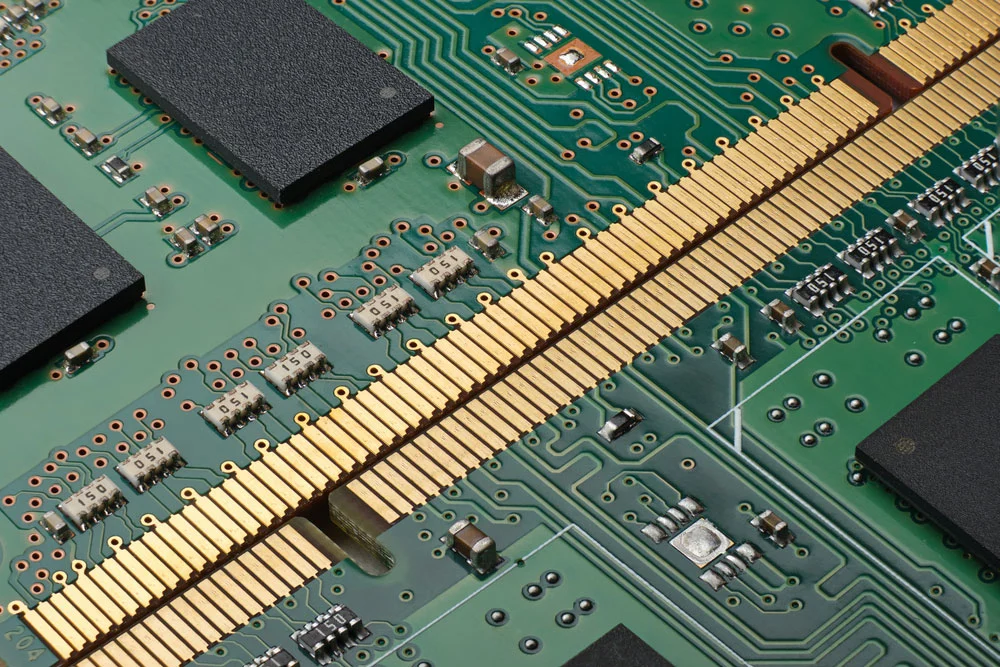
Sometimes, our customer would like to chooses gold plating process for their PCB. So, what is gold plating? What we call the whole board gold plating generally refers to “plated gold”, “Electroplated nickel gold plate”, “electrolytic gold”, “electric gold”, “Electric nickel gold plate”, and there is soft gold and hard gold (usually hard gold is used for gold fingers).
The principle is to dissolve nickel and gold (commonly known as gold salt) in chemical potion, immerse the PCB in the plating tank and connect the current to the circuit board Nickel-gold plating is formed on the surface of copper foil. Electro-nickel-gold is widely used in electronic products because of its high hardness, wear resistance, and resistance to oxidation.
So, how about immersion gold? Immersion gold is formed by a chemical oxidation reduction reaction method, generally it is thicker. It is a method of chemical nickel-gold gold layer deposition method, which can reach thicker gold layers.
2. The difference between gold plating and immersion gold:
A. Generally, the thickness of immersion gold is much thicker than gold plating. The immersion gold will be golden yellow and the color is brighter than gold plating. Therefore, usually customer would be more satisfied with immersion gold. The crystal structure formed by the two process is different too.
B. Because the crystal structure formed by immersion gold and gold plating is different, the solder-ability of immersion gold is better than gold plating, which will not easily cause poor welding. At the same time, because immersion gold is softer than gold plating, thus, the PCB with gold finger are generally use gold-plating, due to the wear-resistant for hard gold.
C. There is only nickel-gold on the pad of the immersion gold PCB. The signal transmission in the skin effect in the copper layer will not affect the signal.
D. The crystal structure of immersion gold is denser than gold plating, and it is not easy to produce oxidation.
E. As the wiring becomes denser, the line width and spacing have reached 3-4 MIL now. Gold plating is prone to short circuit of gold wire. The immersion gold PCB only has nickel gold on the pads, so it will not produce a short circuit easily.
F. The immersion gold PCB has nickel-gold only on the pads, so the combination of solder mask and copper layer on the circuit is stronger. It will not affect the spacing when our engineers make compensation.
G. If you require high requirements for your PCB, and the flatness is better, usually it is better to choose immersion gold process for your PCB, immersion gold generally does not appear black pad phenomenon after assembly. The flatness and standby life of an immersion gold PCB are as good as those of gold plating.
3. What is the the difference between immersion gold and gold plating?
Immersion gold(ENIG) and Electroplated nickel gold
| Immersion Gold(ENIG) | Electroplated Nickel Gold |
| First, a nickel plating layer containing 7-9% phosphorus is formed on the surface of the bare copper of the PCB by reactive deposition,and the thickness is about 3-5um,and then a pure gold layer with a thickness of about 0.05-0.15um is replaced on the nickel surface | Copper/nickel/gold plating is applied to on the bare copper surface of the PCB. The nickel layer is about 4-8um, and the gold layer is about 1-3u" |
| The difference between the mechanism of chemical nickel gold (immersion gold) and electroplated nickel gold (gold plating) is shown in the above table. | |


4. Difference between characteristics of immersion gold plate and gold plating?
Difference between characteristics of immersion gold plate and gold plating
| Surface coating\performance | Apperance | Soldering-ability | Signal transmission | Quality | Engineering |
| Gold plating | Golden blush | Sometimes-welding failure | Skin effect is not conductive to the transmission of high-frequency signals | 1. Gold surface is easy to oxidize 2. It is easy to cause short 3. The welding resistance is not strong | Line width compensation affecting spacing |
| Immersion gold | Golden yellow | Good | Skin impact has no influence on signal | 1. Not easy to be oxidized 2. No gold wire 3. The solder mask has a good binding force | Line width compensation without affecting spacing |

Why We Do Not Recommend Our Customer to Choose HASL
As ICs become more and more integrated, more and more IC pins become denser. However, it is difficult for the HASL process to flatten the thin pads, which brings difficulty to the assembly of the SMT components; in addition, the life-span of the PCB with HASL process is short. The gold plating PCB can solve these problems.
1. For the SMT process, especially for ultra-small surface mount components with the package size of 0603 and 0402, the flatness of the pads is directly related to the quality of the solder paste printing process and has a decisive influence on the quality of subsequent reflow soldering. Therefore, gold plating on the entire board is common in high-density and ultra-small surface-mount processes.
2. In the trial production stage, due to the influence of component procurement and other factors, it is often not that we can assemble the components immediately once the PCB is finished, but often it takes several weeks or even months to start the assembly of components. The life-span of the gold-plating PCB is longer than the PCB with HASL process, so everyone is happy to use them. Besides, the cost of gold-plating PCB in the prototype stage is similar to the HASL process.
3. But as the wiring becomes denser and denser, the line width and pitch have reached 3-4 MIL. So it brings the problem of short circuit of gold wire.
4. As the frequency of signals becomes higher and higher, the effect of signal transmission in multiple coatings due to skin effects will have a more pronounced effect on signal quality.
Skin effect refers to: high-frequency alternating current, the current will tend to concentrate on the surface of the wire.
Frequency(Hz) & Depth(mil)
| Frequency(Hz) | Depth(mil) | Frequency(Hz) | Depth(mil) | Frequency(Hz) | Depth(mil) |
| 60 | 8.6 | 100 | 6.6 | 1k | 2.1 |
| 10k | 0.66 | 100 | 6.6 | 1m | 0.066 |
| 10M | 0.021 | 100M | 0.0066 | 1G | 0.0021 |
Why Choose Immersion Gold Process Instead of a Gold Plating?
1. Because the crystal structure formed by immersion gold and gold plating is different, immersion gold will be golden yellow and the color is brighter than gold plating.
2. Because the crystal structure formed by immersion gold and gold plating is different, immersion gold has better soldering-ability than gold plating, which will not cause poor welding easily.
3. Because the immersion gold PCB only has nickel gold on the pad, the signal transmission in the skin effect is in the copper layer will not affect the signal.
4. Because immersion gold has a denser crystal structure than gold plating, it is not easy to produce oxidation.
5. As the immersion gold plate only has nickel gold on the pads, it will not produce gold wires and cause shortness.
6. Because the immersion gold plate has only nickel gold on the pad, the combination of solder mask and copper layer on the circuit is much stronger.
7. It will not affect the spacing when making compensation.
8. The flatness and life-stand of the immersion gold PCB are as good as circuit board with gold plating finishing.
Any more information about PCB surface finishing features, you are warmly welcome to contact us by service@wellerpcb.com


