Nowadays, time is the most expensive in all. When you finish a new PCB design, next step is to have it manufactured at shortest time, then to perform a couple of complex tests, verification, and approval before getting electronic products to market.
A quickturn around PCB is extremely critical during the prototype verification, pre-production trial, and full production phases of any electronic product containing a printed circuit board. Inconsistent timelines can lead to product delays, hurry and rush testing, ultimately resulting in a poorer quality product to the market.
WELLER offers focus on quick turn PCBs manufacturing services with top quality in first. Everything we do in quick turn printed circuit boards manufacturing is never to be compromising, such as UL listed material, thoroughly via hole copper plating.
What is a Quick Turn PCB
A quickturn PCB means all processes from the design, fabrication, assembly, and testing must be finished at an extremely short time. The quick turnaround time differ from 12 hours to 10 days based on the complexity of the project.
Simply, a two-layer PCB, its manufacturing costs can be kept at a minimum and delivered on a very quick timeline
As complexity increase, PCB fabrication and production will be longer in turn. Keeping these factors in mind is critical to right decision when you plan to have a quick turn PCB requirement for your project.
When Consider Quick Turn PCB Fabrication
There are some benefits why a quickturn PCB service is preferred.
| Expedite the testing and verfication of designs ideasrposes. |
| Get DFM assistance to reduce and optimize the overall project costs and time-to-market. |
| Optimizing product efficacy before running in large-scale production |
| Supports the small quantities production of prototype boards required for design and validation purpose |
WELLER Typical Turnaround Time for Quickturn PCBs
The exact turnaround time depending on many factors such as complexity of the design, material availability, components available in stock, etc.
| PCB Type | Layers | Fab without assembly (days) | Fab and assmelby (days) |
| Standard FR4 | 1-6 | 1-3 | 2-4 |
| Standard FR4 | 8-12 | 3-5 | 5-6 |
| Rigid-flex | 1-12 | 6-8 | 7-9 |
| Flex | 1-10 | 3-6 | 5-7 |
Key Factors that Affect the Turnaround Time of Prototype PCB
Today, there are thousands of printed circuit board manufacturers in the US, Europe and Asia, so it is very easy to have your PCB manufactured at any time per your demand. But there are some key factors on PCB manufacturing that you simply need to know before you begin working on your PCB design. These factors can save your time and cost once considered it into your design.
Circuit board design and test instruction
Follow DFM guidelines to get top quality circuit boards. Check the base material and components availability before using it in your PCB desing and work out the best layout matches for a compact design. Provide specific test requirements and list a clear test equipment beforehand is key for a rapid prototypes.
Lamination Pressing Cycles
An HDI printed circuit board has different types of via strucutres will need multi-lamination cycles. Every cycle you laminate a HDI board, it is like making another multilayer board. It will incease the cost of the PCB. The lead time for advanced technology quickturn boards with multiple lamination process will be longer than that of standard technology printed circuit boards.
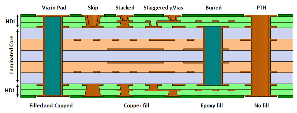
The exact time required for a lamination cycle determined by the number of layers in PCB stack up, and the base material selected. Typcially, each extra added lamination cycle will increased another 3-5 days for the production process. This includes the time taken for any type of hole drilliing, palting, or filling. Eexcept the time take for lamination, another necessary consideration that one additional day needed the out layers process.
For example, the stack up in above picture presents an HDI PCB desinged with stacked via and micro vias. Such an HDI PCB board would have a 2+N+2 stack up, and need a total of 3 lamination cycles, the lead time of such type of board usually would be 10-12 days.
Via-in-PAD Plating
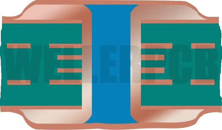
Most time, the designer have to design the via holes in surface mounting PAD, so as to saving the spacing and reduce the PCB overall size, lower PCB layers as well. Or this process may be used to keep heat dissipation from under the component. The manufacturing technology of Via in PAD design become very common now and no challenge to most of PCB manufacturers, but be ware of that they can add one day at least to manufacturing cycle time.
Fabrication Specification and Drawing
A specific PCB fab drawing present important manufacturing information like some critical mechanical dimensions, PCB layers, board thickness, base material, copper thickness, specific layer stack-up, drill chart, surface finishing, the color of solder mask and silkscreen, specific critical tolerance such as press fit holes, controlled impedance details, IPC class 2 or 3, the details of other special requirement such as countersink-holes.
PCB layout engineer need to thoroughly know the PCB manufacturer’s capabilities to bridge the gap between design and design and DFM. For example, the minimum track width/spacing, the spacing between hole and track should be accommodated in the manufacturing process to avoid any re-design time delays.
If no special dielectric thickness requirement, the stack-up must match manufacturer’s standard stack up as possible, these will mean you will get availability of base materials, and get cost down and shorten the lead time accordingly. Once you have to consider a special stack up from impedance purpose, you need to cooperate with the engineer of your supplier to generate a production stack up that they have available materials in stock to avoid any impacts on the lead time once some prepgrege or core is out of stock. Of course, you need to specifically list your impedance requirement(layers, impedance type, impedance value, etc). After all, the less mismatched information, the more possibility to avoid delays.
Suface Finishing
Surface finishing is another time consuming production process. ENIG (Electroless nickel immersion gold) and HAL lead free are the most commonly used surface coatings. Normally, HAL LF takes around 15-30 minutes but ENIG takes 90-130 minutes. Alerts that some PCB manufactures in China do not have ENIG production process at house and need to sub-contract it to outsources with which takes 1 day more on this process.
If your circuit board have edge contacts on and need to be hard gold plated, plus ENIG surface finishing, that means you need multiple surface finishing ENIG + Hard gold plating, then you need to consider twice time of the plating process. As each finishing must be done separately and have to go through the complete process twice.
Assembly Drawings and Notes
A complete assembly drawing will have a right instruction to your PCB assembly manufacturer that how to assembly your board properly. Normally, it includes the specific information such as: BOM list, top and bottom silkscreen, identification label if any, other assembly-specific notes. The assembly drawing along with fab notes will be the good reference to the inspection of the bare printed circuit board and assembly. The following pointes would avoid delays during PCB assembly process:
How to Choose the Right Quicktrun PCB Manufacturer
A good contract manufacturer will ensure you do not compromise on quality over cost and not lose time. Partnering with a qualified manufacturer who can offer prototype PCB manufacturing has many benefits such as delivery on time and quality assurance. CM will have facilities who can provide a stand product with using latest technologies within specific lead time.
Other impact factors need to be considered:
Location: Location is a critical factor to prototype delivery. A local PCB manufacturer will save you much time in communication and shipping. If your budgetary is limited, you can also choose an offshore PCB manufacturer as long as their lead time meet your schedule. Normally, the onshore manufacturer in US or in Europe will have your turnaround time becomes much quicker.
Production lead time: Generally, the manufacturer who only focus on prototype and quick turn production will have more assurance in lead time than that the quickturn around service from traditional mass production manufacturers.
Certification and Qualifications: As that there are a various of manufacturers in the field which offer different quality standard PCBs at big price gap. Make sure that the manufacturer certificated by global quality standards such as ISO, and all materials are UL certificated and applicable in RoHS free, etc.
Consistency: No matter it is prototypes or mass production, make sure your contract manufacturer offer repeatedly good delivery quality boards.
Communication and Support: It is vital that the communication with your contract manufacturer, your manufacturer should be very professional to offer in-depth support in engineering and production. Any your concerning should be addressed immediately.
Above are just some few things to consider before you start prototype productions. To know these factors ahead of time will potentially save your time and cost, also reduce your production time as well. It is important to have a professional quick turn PCB manufacturer to support your prototypes demand.
Why Should You Choose WELLER as Your Ideal Partner?
WELLER, an experienced PCB manufacturer in China, supporting US and Europe customer since 2003, we are more capable of understanding our customer requirement and specification. We focus on IoT, military, medical, telecom, aerospace, automotive, consumer electronics and OEMSs. Our key strengths include:
If you have several projects development every certain times, it is very vital to choose a most efficient and cost-effective manufacturer to make your prototypes. An experienced engineering and skilled manufacturing partner will offer collaborative efforts to that your final product the best per your expectation. Our team at WELLER understand customer design goal and execute their ideas rapidly giving them a competitive advantage.
Let us know freely if you need any design-related assistance, layout issues, stack up design, impedance simulation, etc., our experts will be happy to help you.
Electronics Manufacturing Service
WELLER can help you to expedite your project to market faster with an experienced engineering team major in designing and manufacturing reliable printed circuit boards since 2003. We offer:
If you have a project that hurry to be launch into the marketing and need quick turn PCB manufacturing, components sourcing, PCB assembly and functional testing services, it is critical to find a reliable electronic manufacturing contractor to work with them. Every step from engineering to production will determine the final success.