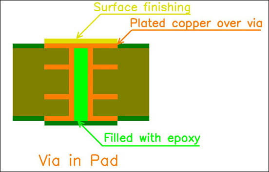
Via in Pad
Due to the increasingly development of new generation electronics from industry 4.0, 5G technology and AI application, more and more electronics devices are smaller and smaller but working on high speed computing, this requires the base circuit board must be load much more components at smallest size than before. Via in Pad is a solution to the challenge of optimizing the printed circuit board size.
What is the Via in Pad in a Printed Circuit Board Layout?
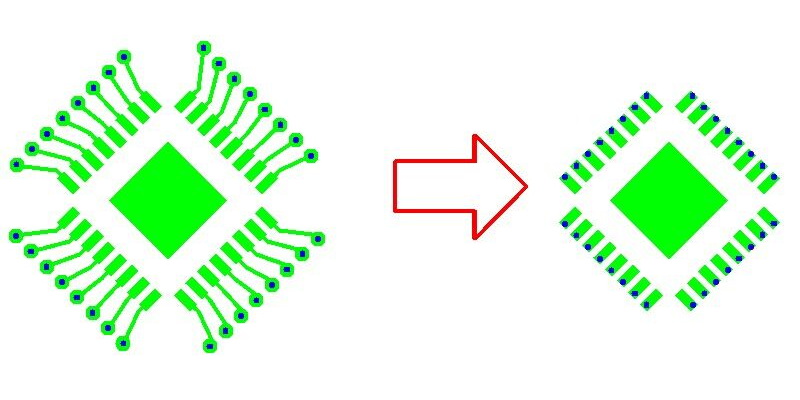
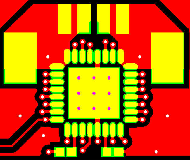
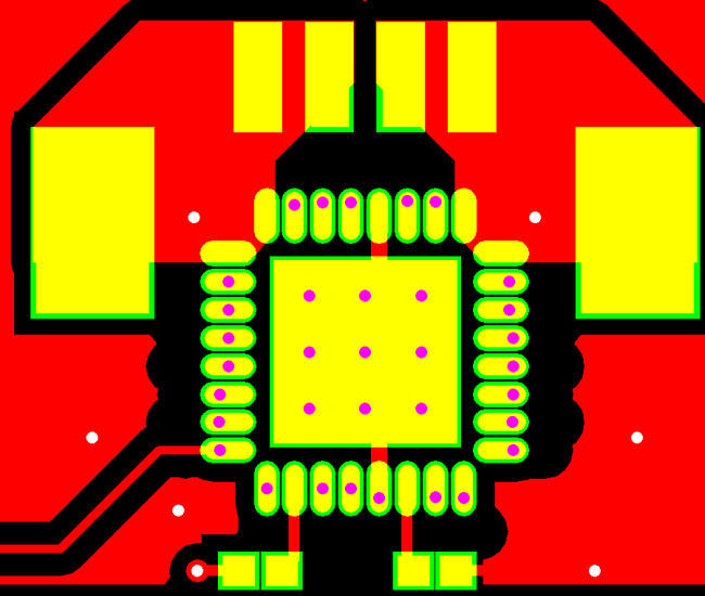
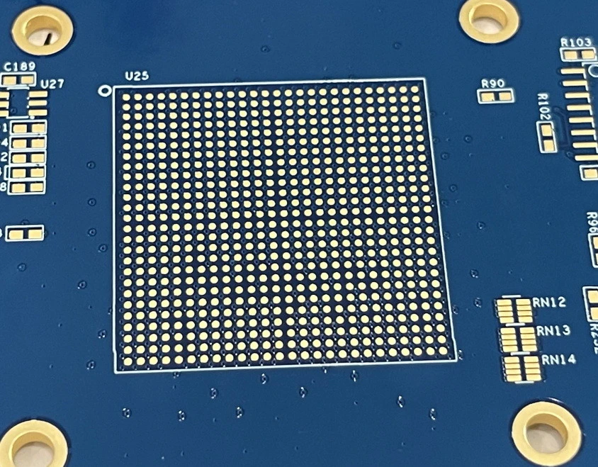
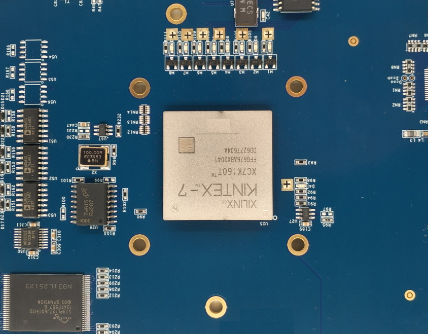
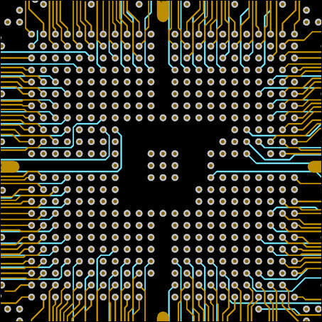
When it comes to PCB layout, or printed circuit board manufacturing, Via in Pad is a special circuit board layout technology to increase PCB density, to allows higher PCB component density (especially in BGA area and SMT IC area). Many electronics engineering designers like to use via in pad technology to significantly save circuit board space so as to load as more components as possible.
How It Looks Like that Via in Pad in an Existing Printed Circuit Board?
When talk via in pad production process in PCB manufacturing process, it is a process to fill the via holes which locate in the solder PAD by resin (conductive or non-conductive), and then plating copper over these holes and it’s pad and then coating surface finishing. This will make sure the finished PAD without any holes to leak the solder pasting in the PCB assembly process. This technology mostly used in some circuit boards with high precise BGA components assembled, or some PCB board with limited smaller over size and over thickness required.
Advantage features of via in pad technology in PCB design
| 1. Via in Pad can optimize trace routing option |
| 2. Via in PAD can help to improve thermal dissipate performance |
| 3. Via in pad can help to reduce inductance in high frequency PCB board. |
| 4. Via in pad can provide a flat surface for SMD component. |
| 5. Can reduce the layer count of a printed circuit board layout |
| 6. Can reduce the over PCB size |
| 7. Can reduce the total PCB thickness |
| 8. Can load much more component at the same area without via in pad design |
Dis-advantage features of via in pad technology in PCB design
| 1. It’s price is high comparing with normal PCB as due to it’s complexity manufacturing process. |
| 2. Risk solder off of the BGA pad if you get low quality. |
| 3. Reliable printed circuit board manufacturer needed. |

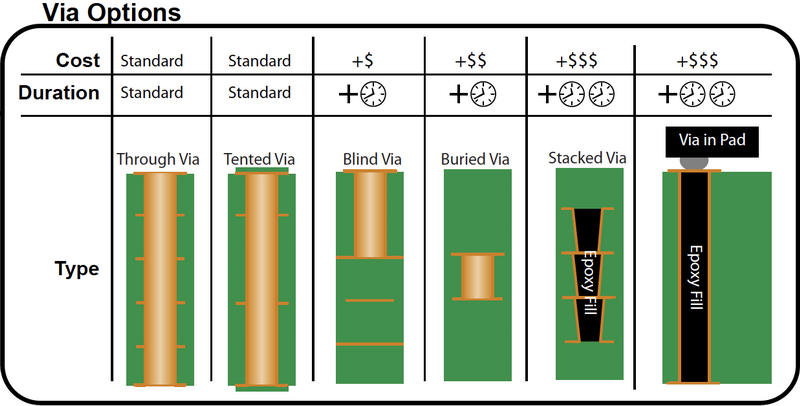
The manufacturing cost reference of Via in PAD technology to traditional via holes
Below is the cost reference from through via holes,tented via holes,blind via holes… to Via in Pad for PCB design reference.
How to achieve the quality of VIA in PAD technology in PCB manufacturing process
Simply 4 steps in via in hole manufacturing process
Step 1: make the via holes as traditional through via holes. Step 2: filling the via holes by resin(conductive resin or non-conducive resin). Step 3: Plating copper over top side(or both side) of the via holes and it’s Pads, to make sure the via hole to be plated as “shut up”. Step 4: Surface finishing treatment over the Pad. |
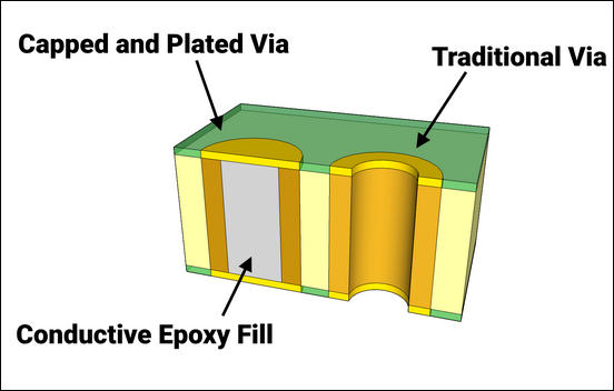
Via in PAD VS traditional via holes:
The PCB design guidelines on Via-in-pad
Following the design suggestion below or contact us freely when you need to perform a PCB layout on via in pad type.
| Via hole size (mm) | PAD size (mm) | Annular ring size (mm) per side |
| 0.20 | 0.40 | 0.10 |
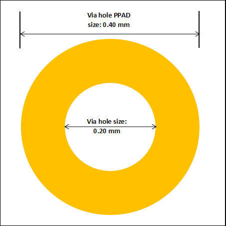
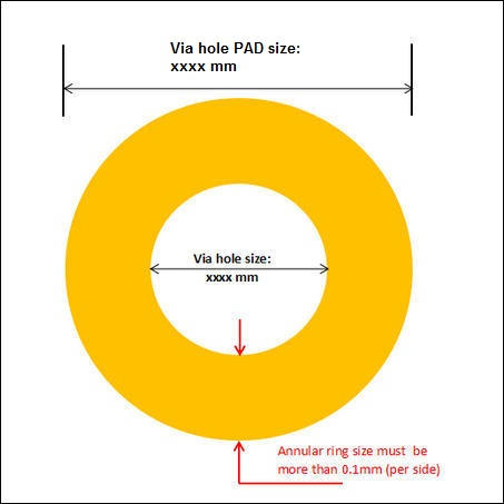
Remark: No matter how big size of your via holes and PAD size is, but the minimum annular ring size must be no less than 0.1mm per side.
For more knowledge about Via in PAD PCB design, you can contact us freely by email: service@wellerpcb.com, our engineer will provide professional consult to your design issues.