Embedded Copper Coin PCB
As the technology in the electronic design and manufacturing is increasingly updated at an exponential rate, and much more integrated circuits applied in the electronic devices around us, the solution to the thermal management is becoming more and more important at bard printed circuit board and it’s PCB assembly filed. Whatever it is high watt efficiency in LED application, a high power transmitter in communication filed, or a high voltage power supply in telecom satiation, the demand for cooling and better heat dissipation is ever seriously increasing.
Normally the heat generated from two factors: one is the outside temperature, the other is the electronic device itself heat, which will take positive impact to the operation performance, reliability, and increased lifespan of the crucial components.
Generally, the goal of thermal management on the bare PCB and printed circuit board assembly is to directly move the heat-generating components to thermal interface materials such as an external heat sink to control the heat.
The Options of Dissipating Heat on Printed Circuit Board
Generally, there are 3 options below to dissipate the head from a printed circuit board:
| Option 1: Via holes filled by resin (Via in PAD)–common performance |
| Specification to holes: 1. Via hole size: 0.2-0.4mm. 2. Though via holes. 3. Via holes plugged by resin and copper plating over on top and bottom side. |
| Option 2: Via holes filled by copper–common performance |
| Specification to holes: 1. Through via hole size: 0.3-0.4mm. 2. Blind via holes: 0.10mm. 3. Through via holes or blind via holes fully filled by copper. |
| Option 3: Cavity or routing zone embedded by copper coin–greater performance |
| Specification to Copper coin: 1. Size: 3.000 X 3.00mm (min); 60.00 X 80.00mm(max). 2. Copper coin thickness: 1-3mm. 3. PCB surface finishing: immersion gold (must be this type of finishing). |
Above options 1 and 2 is a traditional thermal management solution which applied on the general electronic devices which do not require high heat dissipation performance. A higher thermal management (option 3) demand needs the solution presents in below article.
Metal Core Printed Circuit Board- MCPCB
A common way to manage the heat of an electronic circuit board is to directly change the PCB base material from FR4 to metal core as a replacement; we call it as Metal Core Printed Circuit Board- MCPCB. Which is a conductive copper foil layer bonded on a metal plate core via thermal interface material between them. The metal core is usually designed to draw the thermal generated by the active components through the conductive layer and release the heat away by itself. This will greatly increase the thermal performance of a circuit board. MCPCB technology can be composed as a single conductive layer over a metallic base or as a multilayer PCB on the top and bottom sides of the metallic base.
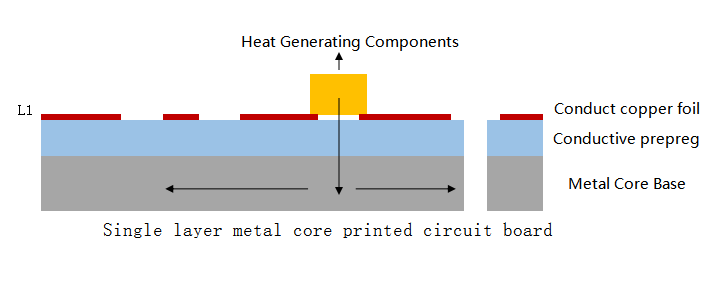
Below is a single layer metal base printed circuit board stackup, which is most commonly used in LED lighting.
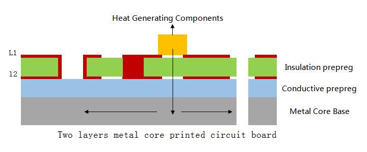
Below is a two layers MCPCB stack-up that presents the dissipation of heat from the surface mount component through the buildup to the base metal plate. This design can offer excellent thermal conductivity of up to 12 W/mK to most electronic devices, but never greater performance than this value. For reaching a higher thermal conductivity result, another technology such as copper pedestal or copper coin is commonly recommended and adopted solution by most electronic designers.

The Increasingly Growing Technology of Copper Coin Printed Circuit Board
In this article we would like to have a deeper discussion about growing technology of copper coin printed circuit boards. Where there is high thermal conductivity material used, there is a heat occurring. Copper as a common conductivity material has it’s excellent property of conductivity up to 380W/mK, plus its reasonable cost and easy to get, the advantages with no other thermal conductive material can replace it. Therefore, it is not an exaggeration to say that copper absolutely is one of the best options to well manage heat while keeping electrical and or thermal conductivity.
The copper coin PCB is the copper coin or copper block embedded or inserted into the PCB Cavity or slot after routing and metalized when finished printed circuit board lamination. PCB and it’s copper coin tightly connected. Typically the copper coin locates under the high heat-generating component(s) which need to be cooled. Compared with a via farm, copper coin can greatly provide about twice the cooling. And optimizing solution by using thermally conductive material, the copper coin can be directly contacted between the heat-generating component pad to the heat sink. Copper’s thermal conduciveness is on average 20-200 times greater than any other conductive dielectric prepreg out there.
When you design an electronic device, if there is a specific or some components on a printed circuit board that are for the most sources of high heat generated and heat dissipation by via holes cannot support that, copper coin technology is best solution to thermal management.
Copper coin is providing the ultimate heat transfer solution in a specific zone on a printed circuit board no matter the number of layers of the board or the PCB base material. Basically, it is to get a copper coin embedded or pressed fit into a cutout or cavity in a printed circuit board right under a zone that is specified as a heat source, then the heat is directly transferred to a heat sink via the circuit board stack up. Obviously that the heat do not pass through PCB buildup materials that have disadvantages in thermal management and bottleneck in heat dissipation
How to embed the copper coin into the PCB can be manufactured in different shapes and configurations. Normally the designer make a design on the configuration by the balance between routing, power plane requirement and proximity of the copper coin to the component that needs to be heat dissipated.
After all, copper coin is a relatively new technology and still under upgrading, much success already seen but some hard nuts are still under study by related engineering and production developers. Any time you’re putting a copper coin into a PCB stack-up, some factors such as registration, tolerances will become a necessary concern and there would be a greater need for process control. At present, copper coin as new thermal transfer solution has been efficiently applied to at the bare PCB manufacturing and production. Whether you are working on a metal core printed circuit board design or a copper coin PCB design, we strongly recommend always consulting and working with your PCB manufacturer, particularly with these outstanding new technologies.
Need more information about copper coins?
Please feel freely to contact our experts for guidelines and support with any projects you have.
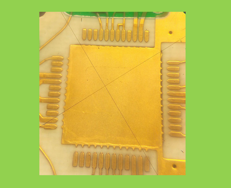
How to manufacture copper coin embedded PCB.
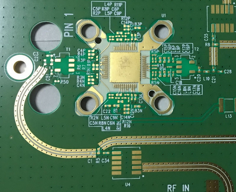
PCB with embedded copper coin and RFI metal backed