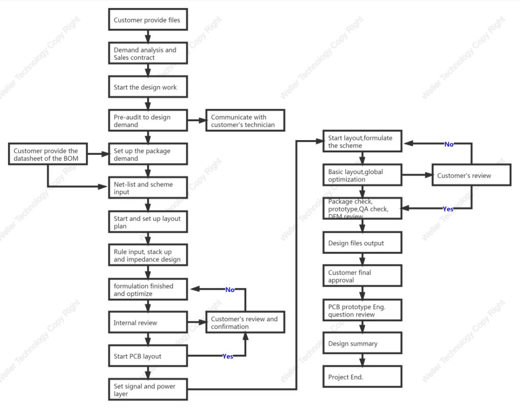
PCB Design Layout Process
Good work on PCB layout will directly improve the final PCB manufacturing yield, as well as price optimized. All the printed circuit board design layout process at Weller follow ISO9001 work flow as below:
What Software WELLER Use For PCB Layout
It depends on customer’s needs, both popular PCB layout design softwares Altium Designer and Cadence Allegro are available to WELLER. We can submit efficient PCB layout work as quick as 12 hours.
Altium Designer
Our engineers who is professional in Altium Designer can delivery complexity layout work as quick as 24 hours.
Cadence Allegro
Our engineers who is professional in Altium Designer can delivery complexity layout work as quick as 24 hours.