WHAT IS A PCB TRACE WIDTH CALCULATOR?
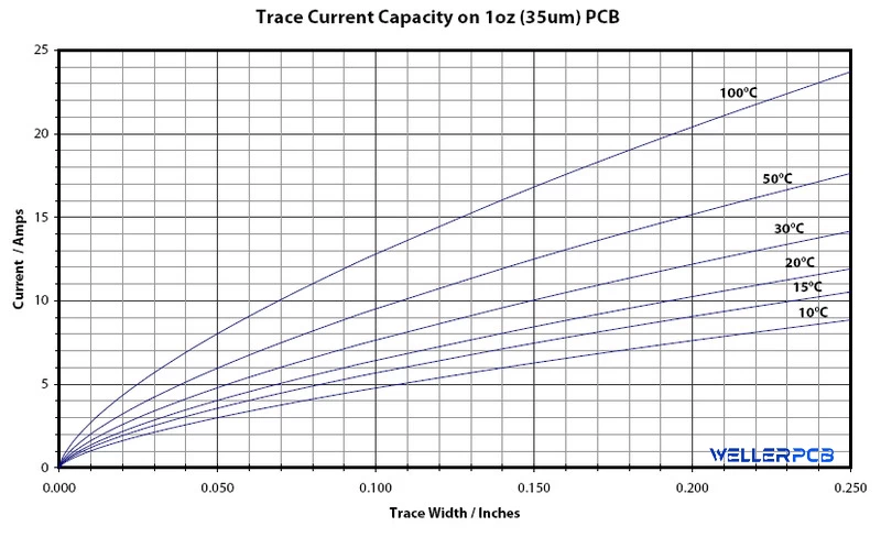
While you start a PCB design, this PCB trace calculator will help you to get the copper weight and circuit trace width.
You can use our calculator to determine various printed circuit board trace components, such as trace temperature, maximum current, resistance, voltage drop and power dissipation. You can better understand your calculator results by becoming familiar with the following formulas.

Max Current
Generally, You can use this formulate as a reference to calculate the maximum current: A=(T x W x 1.378 [mils/oz/ft2])
The values in this formula correspond with the following parameters:
A: Cross-section area.
[mils2] T: Trace thickness.
[oz/ft2] W: Trace width.
If you have worked through the previous equation, you’ll determine the maximum current by using formulate: I IMAX = (k x TRISEb) x Ac.
The fields for this formula are as follows:
[mils] IMAX: Maximum current.
[A] TRISE: Maximum desired temperature rise.
[°C] k, b and c: Constants.
Trace Temperature
PCB Trace temperature is another important parameter in calculating circuit trace width. The formula for determining trace temperature is : TTEMP = TRISE + TAMB.
Determining PCB circuit trace temperature requires nothing more than three total parameters. The values read as follows and are calculated in Celsius:
TTEMP: Trace temperature.
TRISE: Maximum desired temperature rise.
TAMB: Ambient temperature
Resistance Calculation
When calculating circuit trace resistance in your printed circuit boards, you’ll begin by converting the cross-section area from [mils2] to [cm2] following the formula A’ = A * 2.54 * 2.54 * 10-6.
After working through the equation, you need to quantify the trace resistance by using formula R = (ρ * L / A’) * (1 + α * (TTEMP – 25 °C).
Exactly the values in these formulas correspond with the following quantities:
T: Trace thickness.
[oz/ft2] W: Trace width.
[mils] R: Trace resistance.
[Ω] ρ: Resistivity parameter.
[Ω · cm] L: Trace length.
[cm] α: Resistivity temperature coefficient.
[[1/°C] TTEMP: Trace temperature.
Voltage Drop Calculation
PCB Voltage drop is the decrease of electrical potential as it moves through a current in an electrical circuit board. The equation for determining voltage drop is VDROP = I * R.
The three values in this formula are as below:
VDROP: Voltage drop.
[V] I: Maximum current.
[A] R: Trace resistance.
Power Dissipation Calculation
Circuit power dissipation occurs when an electrical device operating generates heat, resulting in energy loss or waste. It is calculated by using the formula PLOSS = R * I2.
Each of these quantities should be reads as follows:
PLOSS: Power loss.
[W] R: Resistance.
[Ω] I: Maximum current
FAQS ABOUT CALCULATING PCB TRACE WIDTH
Actually, calculating printed circuit board trace is exactly a confusing process for those who are new designer to using trace thickness calculators. If you have questions regarding this calculator, the formulas or your calculating results, you might freely find an answer in the following FAQs:
“Mil” gets its name from the Latin term, “mille,” meaning “thousand.” A mil is one one-thousandth of an inch.
Temperature rise is the difference between your PCB’s maximum safeoperating temperature and its usual operating temperature.
Yes. Based on the formulas, the tool can only calculate trace width of up to 400 mils, 35 amps, copper of 0.5 to 3 ounces per square foot and a temperature rise between 10 and 100 degrees Celsius. The calculator will extrapolate the data when used outside these ranges.
External trace layers have a high heat transfer, while internal layers do not conduct heat as well, meaning internal traces can store more heat.
Use Our Services For Your High Quality PCB Fabrication
After all, the PCB trace size calculator above as only a reference to your electronic product design. All final circuit trace size is upon designer global knowledge and complete understanding on his designed projects, IPC-D-275 would be a better and official reference of designing trace size.
Track width design for 1 oz copper PCB
| Current/A | Track Width(mil) | Track Width(mm) |
| 1 | 10 | 0.25 |
| 2 | 30 | 0.76 |
| 3 | 50 | 1.27 |
| 4 | 80 | 2.03 |
| 5 | 110 | 2.79 |
| 6 | 150 | 3.81 |
| 7 | 180 | 4.57 |
| 8 | 220 | 5.59 |
| 9 | 260 | 6.60 |
| 10 | 300 | 7.62 |
| IPC-D-275 Recommended Track width For 1 oz copper PCB and 10 °C Temperature Rise | ||
When you start a PCB layout work, specially for some high current power supply management PCB, it is necessary to have a correct track width calculation upon your max running current, or else, the circuit board could be burned once high current loaded on. Or, you can contact us for a professional PCB layout service.


