PCB Reverse Engineering
When you have an old electronics board which without any backup files (Gerber, BOM list, Schematic drawing, CAD file), but you must need repeat production for new and important demand. The pervious manufacturer is also lost. If you do not want to scrap the system that related with this circuit board, the only option is to re-build this electronic circuit board (including PCB layout, circuit board fabrication, turnkey PCB assembly, firmware injection and functional testing, etc.). Even for an experienced layout company this process is a hard work and real challenge.
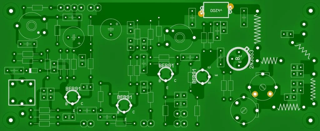
PCB to PCB Layout to Schematic Reverse
However, as a real experienced team at professionalism more than 10 years, WELLER is able to convert any printed circuit boards into schematic diagram. We can provide complete parts list, components values, package and other data. If you want to change any physical printed circuit board into schematic, our full services as below is available for you at any time.
| Schematic Diagram Creating |
| PCB Design |
| PCB Layout |
| BOM Generating |
| Pick and Place File Generate |
| Chip Decryption |
Schematic diagram copy is reverse engineering of PCB that is commonly used to the changing in printed circuit diagram design for better to work. Through this process we can obtain all the necessary information about the printed circuit boards and get the correct schematic diagram for purpose of copy a design through printed circuit board file or directly route it according to physical PCB sample.

Reverse Engineering Process
Only Focusing on 100% Accurate and Proven Process
Need electrical data? Lost your CAD-generated design & fab files and no backup? Need a schematic drawing for repair or debug? Need to re-engineer a legacy printed circuit board to data that has exact FORM, FIT and FUNCTION? WELLER Technology has a capable of offering all the needed products and/or services to complete the fully re-engineering of an assembled PCBA all the way back to schematics & Netlist!
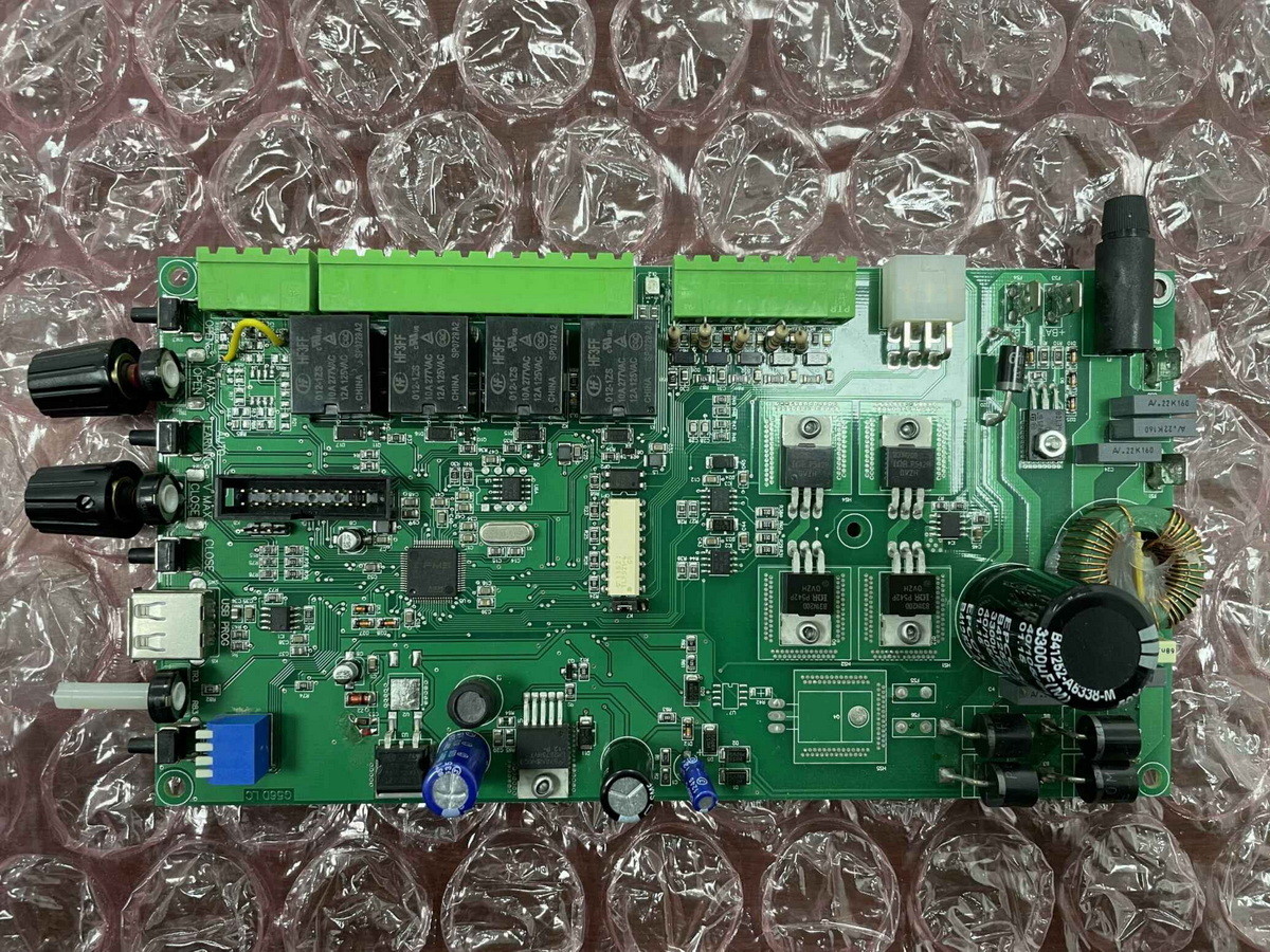
Original old PCB

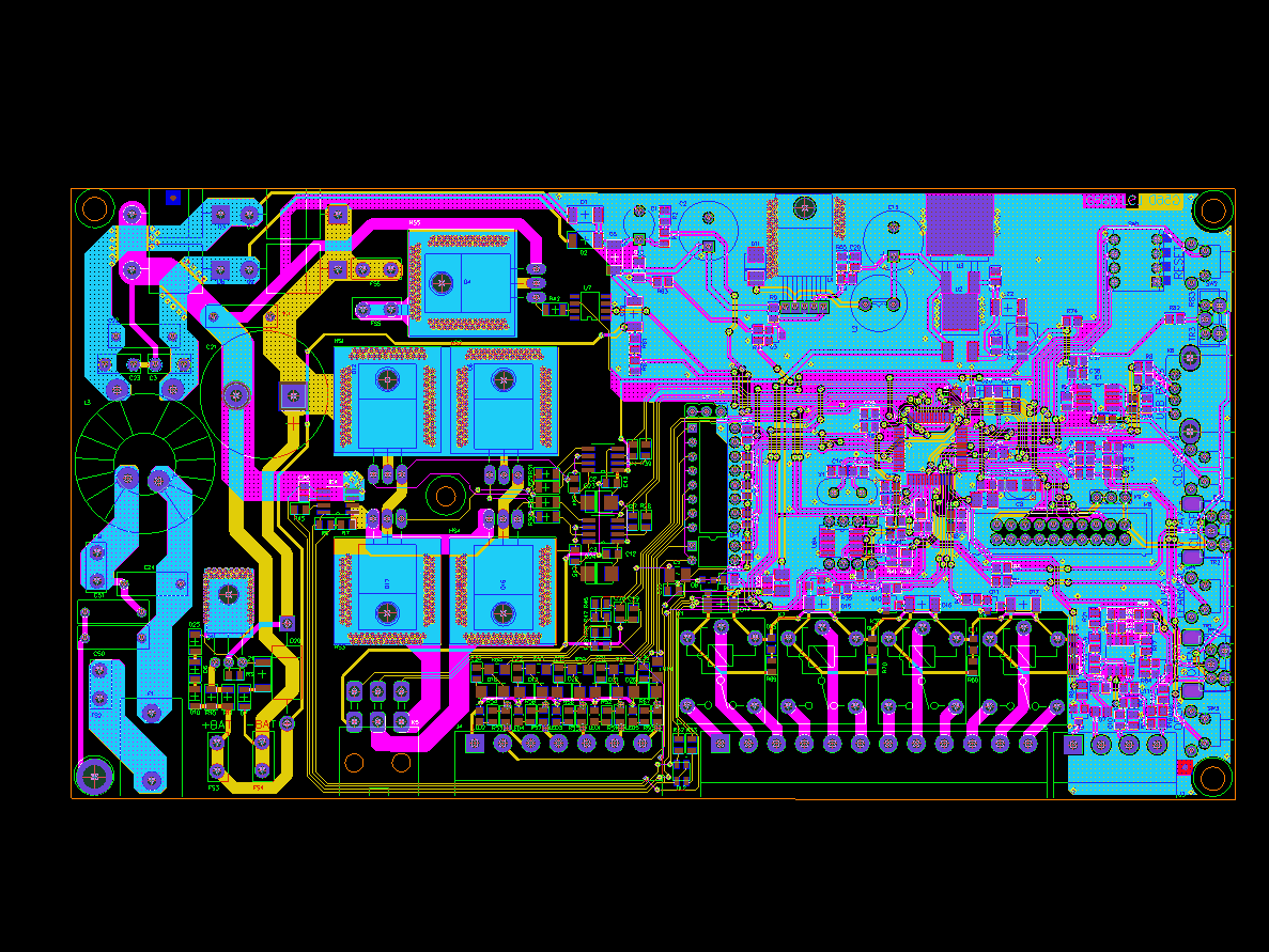
Reverse Gerber file

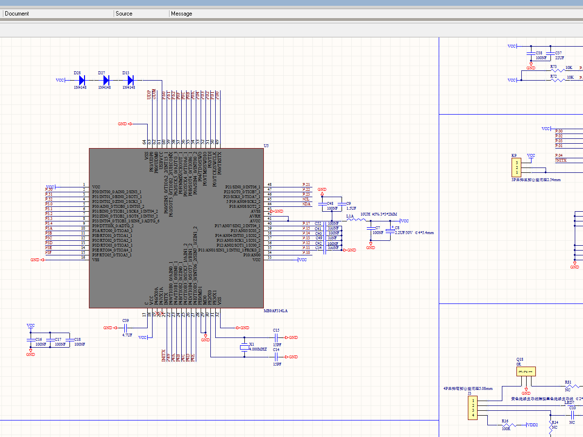
Schematic drawing creating
Instead of bearing a long and expensive redesign process, directly ask WELLER Technology to produce the necessary data for your demand. The process of image capture in black and white, gray or color through the conversion of raster to vector data by several quality control steps and finally the output in a wide variety of formats is all work finished in a logical, intuitive and well-designed platform.
Expertise
Absolutely that is an extremely complex and difficult work with requiring great care and experience to convert a PCB to schematic. Our experienced team will do the following work at highly concentrated and skilled manner.
| Copy an obsolete printed circuit board (PCB copy). |
| Re-create lost or missing PCB manufacturing files. |
| Update an existing populated PCB with new capabilities. |
| Re-engineer an old PCB design to current standards, compatible to new components. |
| Re-engineering for cost saving/obsolescence. |
Frequently Asked Questions
About PCBA Reverse Engineering Cost and Work?
1. In general, it is necessary to provide the exact PCBA picture with viewing from top and bottom side separately, and the size of the circuit board.
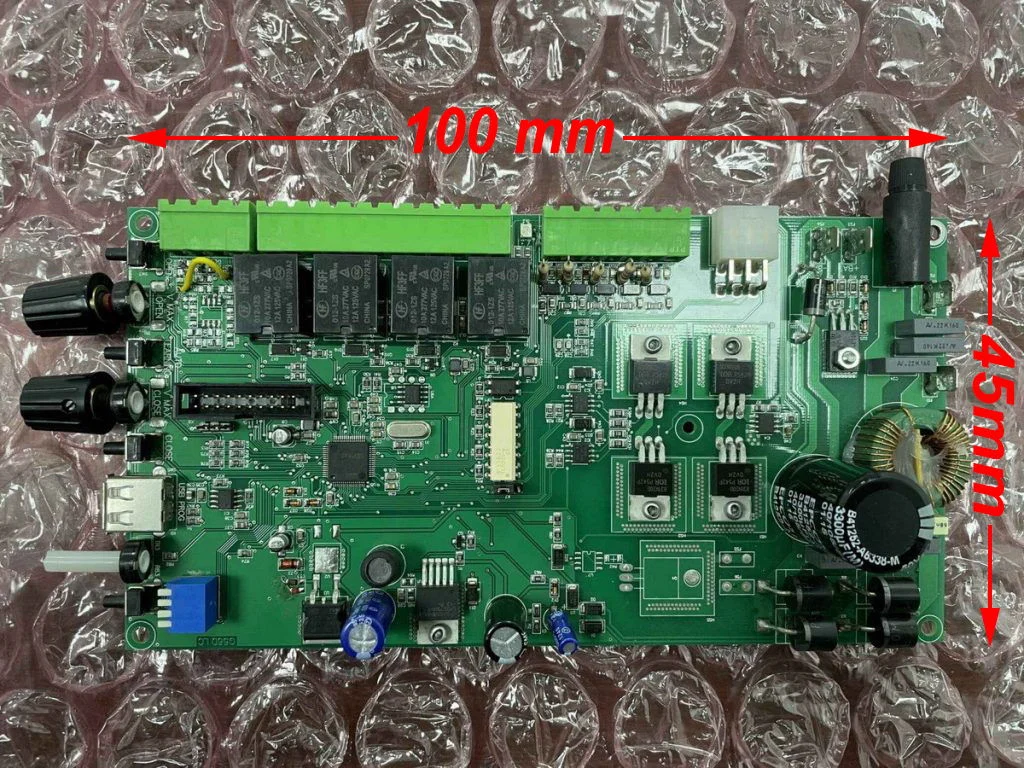
2. For some special or complex PCBA board, we may need an existing PCBA to have an actual evaluation.
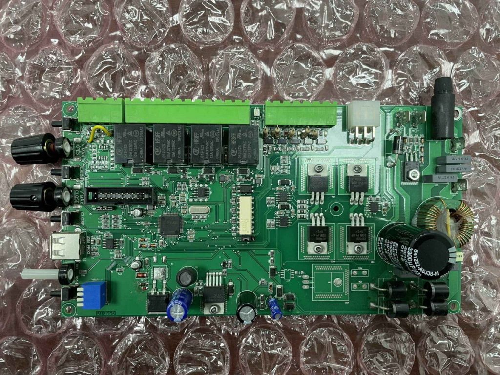
1. 1 pcs PCBA board with fully functionality and stable performance. (The below picture is an example PCBA ready for reversing engineering).
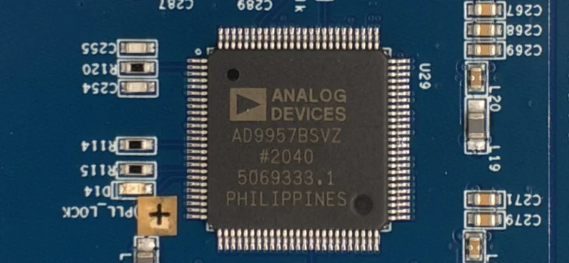
2. In addition to common and generic capacitors and resistors; the silkscreen for some critical complements (such as ICs (chips), diodes and transistors, etc) on the PCBA board should be complete for viewing (the example as shown below for U29).
