
When electronic engineers create printed circuit boards (PCBs), they tend to leave many copper-free areas on the board. They are probably not aware of the technicalities of the PCB production process. A high percentage of the copper-free area on the board can have a negative impact on the product and leave it susceptible to early damage.
That’s where copper pouring comes into play. In this blog, we will explain why PCB copper pouring is such an important step in the printed circuit board production process. If you think, like many other novices, that less copper pouring means reduced cost, you are sadly off the mark. It’s true that the area of electroplating becomes smaller, and you may save copper too.
However, good PCB manufacturers always place quality on top priority. When it comes to producing PCBs, copper pouring in adequate measure boosts the quality of the product.
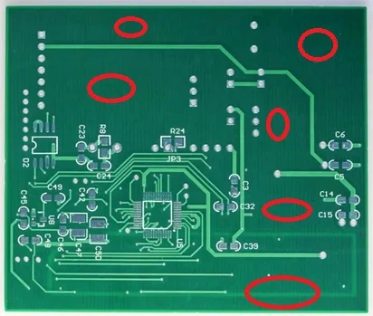
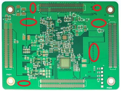
What Happens When The Outer Layer Of The PCB Is Copper-Free?
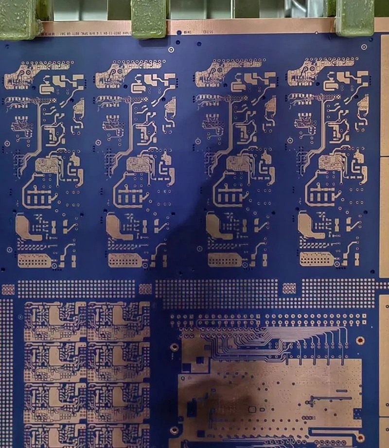
When the PCB board is placed in the electroplating tank, and the appropriate current is applied (refer below fig 1), the PCB appears the physical status after dry film covering.
01: Problem at Outer Layers Copper-Free Area
Affected range: double-sided board, multi-layer board (4 layers and above).
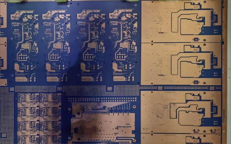
The circuit tracks that exposed from outside of the dry film will be plated by the copper from electrolytic plating tank after current applied to (as shown in fig2).

The total area of the partial circuit exposed outside the dry film will impact the value of the current distribution during the electroplating process. The current received will be more uniform if the exposed copper area is large and the current input is uniform (refer fig3 below). Therefore, the copper plane must be placed on a large area during design to prevent this.
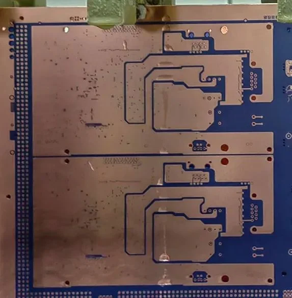
If the total plated area of the copper is too small or the pattern distribution is very uneven (refer figure 4), the current received will also be uneven. Thus, as the current is energized, the greater the current, the thicker the copper plating (The result from this design is that the finished copper thickness could be 2OZ if you request 1OZ only).

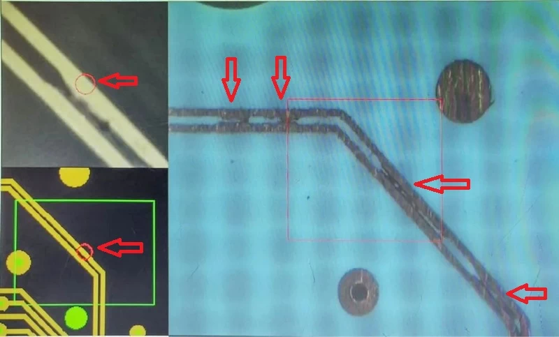
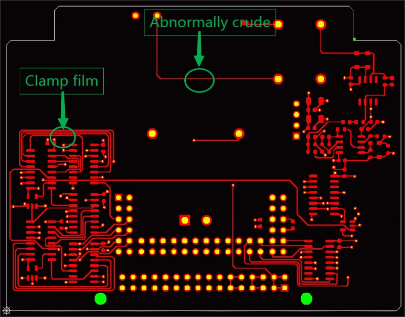
If the gap between the circuit trace is just too small such as around 3mil to 3.5mil, it will create a ‘clamp film’ between the trace. In other words, the dry film is sandwiched in the middle of the gaps. It will result in the subsequent base-started copper being in the middle. If the etching is not cleaned during the process, it can result in a short circuit. (figure 6 and figure 7 ).

Solution:
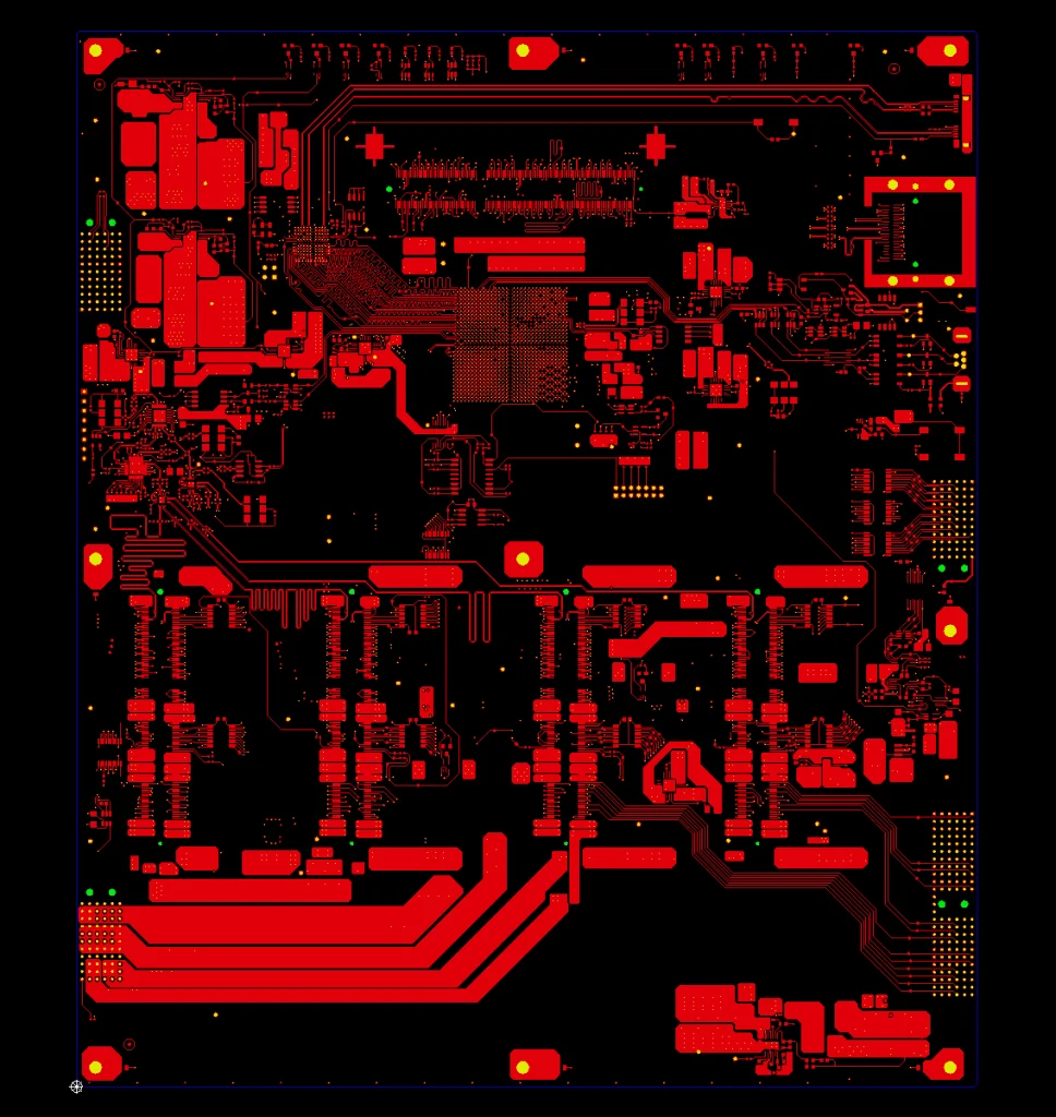
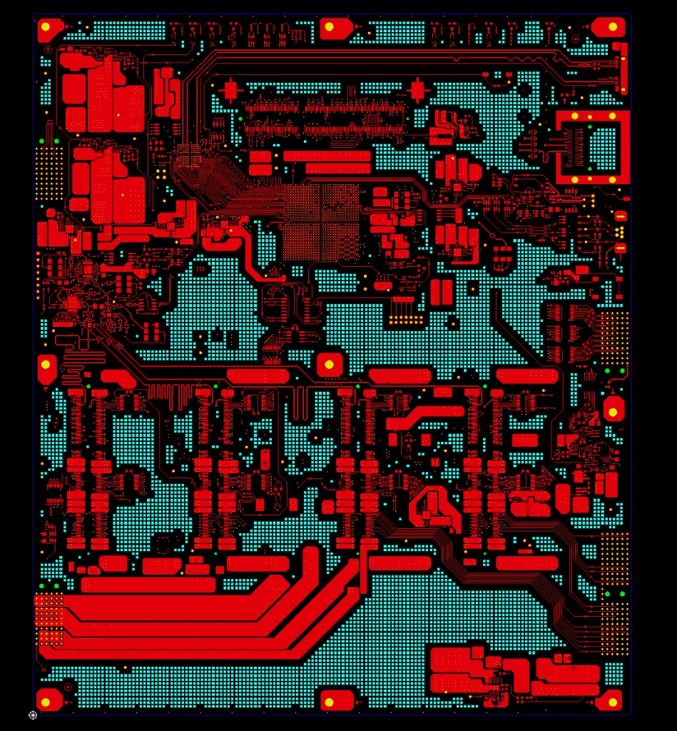
To maintain high quality of printed circuit manufacturing, independent lines must be avoided as much as possible in the PCB design and layout. Also, liberal use of copper is recommended on the entire circuit board. If there are independent lines where it is not possible to pour copper, the gap between the traces must be made as wide as possible.
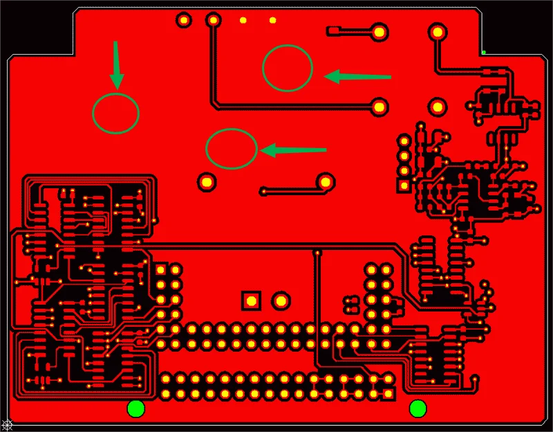
Case comparison before and after improvement:
1.Pouring copper partly
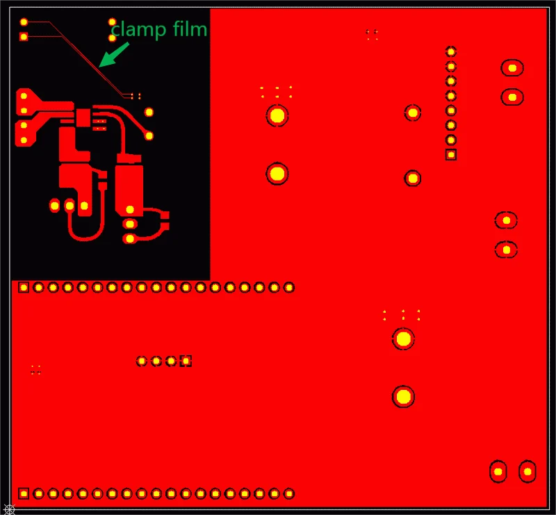
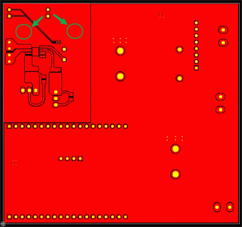
2. Large area without pouring copper
3. Pouring copper by dummy PAD
02 Problem: Problem at Inner Layers Copper-Free Area
Affected Range: Multi-layer board (4 layers and above).
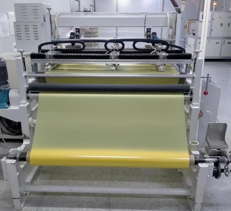
The lamination process of multi-layer printed circuit board manufacturing is to cut PP into sheets. And then they are placed between the inner cores and the outer copper foil and passed through the high temperature and high pressure of the press. In this process, the resin gets melted on the PP and fills the core board on the copper-free area. The resin solidifies after cooling, allowing for the bonding of core of boards and copper foil.
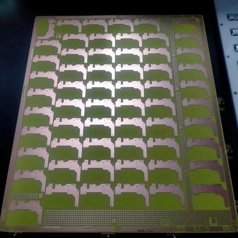
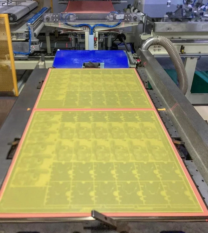
1. When the copper-free area is too large on the inner layers, there will be an excess of resin on the PP and it will flow to the copper-free area. This can result in thinner boards, wrinkled copper skin, white spots, and de-lamination caused by a dearth of resin.

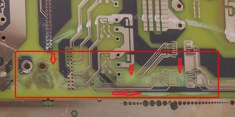
The case is as follows:


2. If the inner copper area corresponding to the gold finger is relatively free, it will create problems such as inadequate thickness in the gold finger area and ineffective contact between the board and the connector slot.

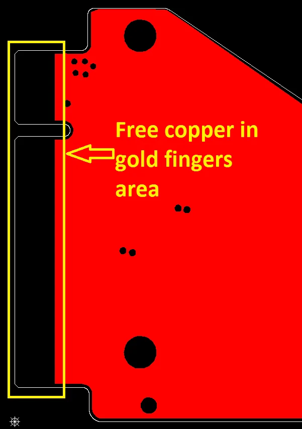

For The Gold Finger Printed Circuit Board:
Copper must be poured on the inner circuit area under the gold finger. The board thickness specifications are also stringent. For the laminated structure, avoid choosing a structure with a lower limit for the thickness of the finished product. The thickness of the finished product is indicated by the number of laminated structures used.
In multi-layer boards, copper is placed in the open area of the inner layer primarily to increase the copper area and reduce the filling area. This ensures the lamination’s reliability and the finished board’s thickness tolerance. Copper is used in the opening area of the outer layer essentially to balance the electroplating current, avoid film clamping and thin lines, and provide more uniformity to the surface copper thickness.
03 Summary Of The Design Rules
As a professional printed circuit boards manufacturer, we have been keeping continuous improving our engineering and manufacturing capability to accommodate latest high technology PCB manufacturing requirement, you can contact us at any time for a free quote.


