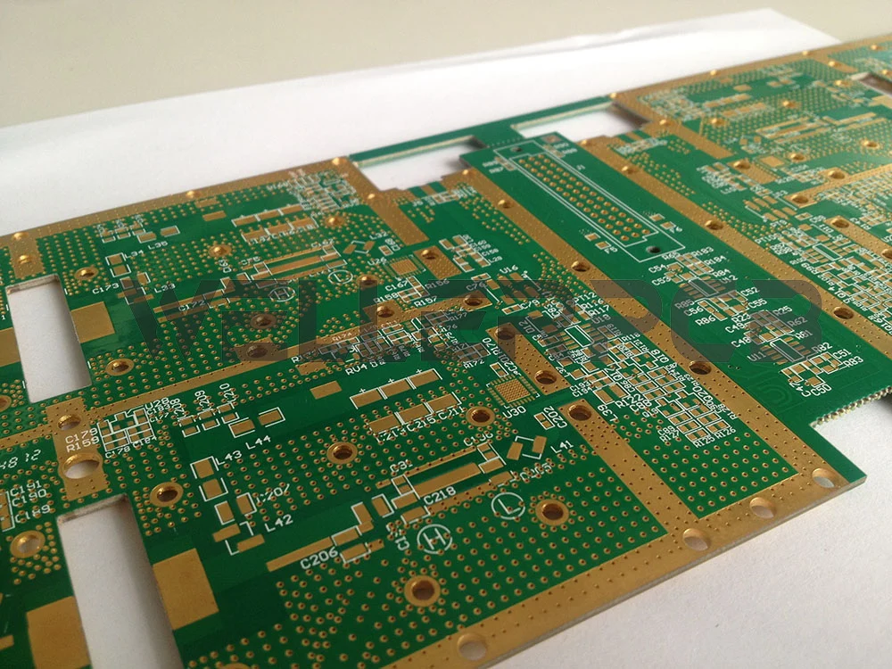
PCB surface finishing technology

When surface finish (also called surface coating) defined to a PCB it means an intermetallic joint between the exposed bare copper of the solder-able area of the circuit board and the electronic components, this excluding the area of solder mask. Printed circuit boards without a protective coating would be susceptible to oxidation, therefore the requirement of the surface finish.

2024/07/Advanced-Immersion-gold-PCB-manufacturer.webp

The application purpose of surface finishing

For soldering: the coating layer can protect the exposed copper area used for soldering from oxidizing.

For durable connectivity feature: Gold connect fingers.

For wire soldering: Wire bonding technology.

The core application of surface finishing

For soldering: The coating layer can protect the exposed copper area used for soldering from oxidizing.

For durable connectivity feature (Gold connect fingers).

For wire soldering (Wire bonding technology).

Two common types of surface finishing

This is to drop the PCB into a batch of molten Sn/Pb solder so that all the exposed cooper to be covered and excess solder is moved by passing the PCB between 230℃ hot air knives.

2024/07/Advanced-HAL-PCB-Manufacturer.webp

Key production parameters of HAL finishing.

(1). Sn/Pb=63/37 (by weight).

(2). The coating thickness > 3um.

(3). Avoid generating non-solderable element Cu3Sn. Cu3Sn come out due to the lack of Sn, for example, if the coating thickness of Sn/PB is too thin, the solder joints changed to non-solderable composition of Cu3Sn from solderable composition of Cu6Sn5-Cu4Sn3-Cu3Sn2.

Production process flow

Removal of anti-etching resist->cleaning of board surface-> printing of solder mask and characters->cleaning treatment-> fluxing ->hot air leveling ->cleaning treatment.

Advantages:

(1). Low Cost

(2). Widely Available

(3). Re-workable

(4). Excellent Shelf Life

Disadvantages:

(1). Un-even Surfaces

(2). Not Good for Fine Pitch Design

(3). Contains Lead (HASL)-unfriendly to environment

(4). Thermal Shock

(5). Solder Bridging

(6). Plugged or Reduced PTH’s (Plated Through Holes)

Free-PCB(Printed-Circuit-board)-stackup-design-support

ENIG: Electroless Nickel Immersion Gold

Chemical Ni/Au refers to electroless Ni plating (thickness ≥3um) on the exposed PCB connection pad and then plating a layer of 0.05-0.15um thin gold over it, or plating a layer of thick gold (0.3-0.5um). Due to the chemical plating layer has very good feature of evenness, perfect smooth surface, and can provide multiple welding performances and the low contact resistance, therefore ENIG is mostly preferred by PCB assemblers due to it’s high electrical conductivity.

2024/07/Advanced-Immersion-gold-PCB-manufacturer.webp

Advantages:

(1). Flat Surface

(2). No Pb (Restriction of Hazardous Substances (RoHS) compliant)

(4). Long Shelf Life

(3). Good for PTH (Plated Through Holes)

Disadvantages:

(1). Expensive

(2). Not Re-workable

(3). Black Pad / Black Nickel

(4). Damage from ET

(5). Signal Loss (RF)

(6). Complicated Process

Free-PCB(Printed-Circuit-board)-stackup-design-support