A printed circuit board (PCB) looks like a multi-layered cake or lasagna or layers of different materials are laminated together by heat and adhesive in the PCB fabrication process. Roughly, 85 out of 100 modern-day electronic devices or products makes use of PCB which brings about its importance in the electrical world. Also, with PCB circuits production in large amounts is faster and at a lower cost unlike with other wiring processes because all the components are put together and attached at the same time.
Generally, the PCB base material of FR4 is made of glass. In most cases, the glass fibre substrate of PCB generally refers to the material “FR4”, which is a type of solid material can provide PCB hardness and thickness.
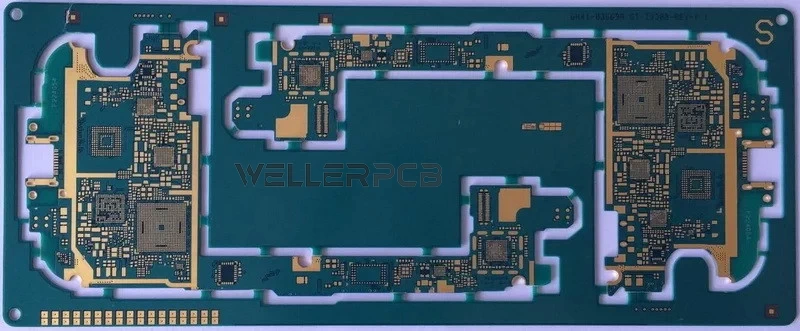
In addition to the FR4 substrate, there are flexible circuit boards produced on flexible high temperature plastics (polyimide or similar), etc. In the PCB manufacturing and production process, the copper foil layer is pressed onto the substrate using heat and an adhesive. In some low cost occasions, PCBs can be single-layered (one copper foil layer) where copper foil may only be pressed on one side of the substrate. PCB can also be two-layered or multi-layered depending on how many copper materials/foils layers that are present in it. Two-layered PCB as the name implies means it has two copper foil layers and multi-layered PCB meaning it has three or more copper foil layers. Of course, in different PCB designs, the number of copper foils may be as little as 1 layer, or more than 16 layers (more details as we proceed).
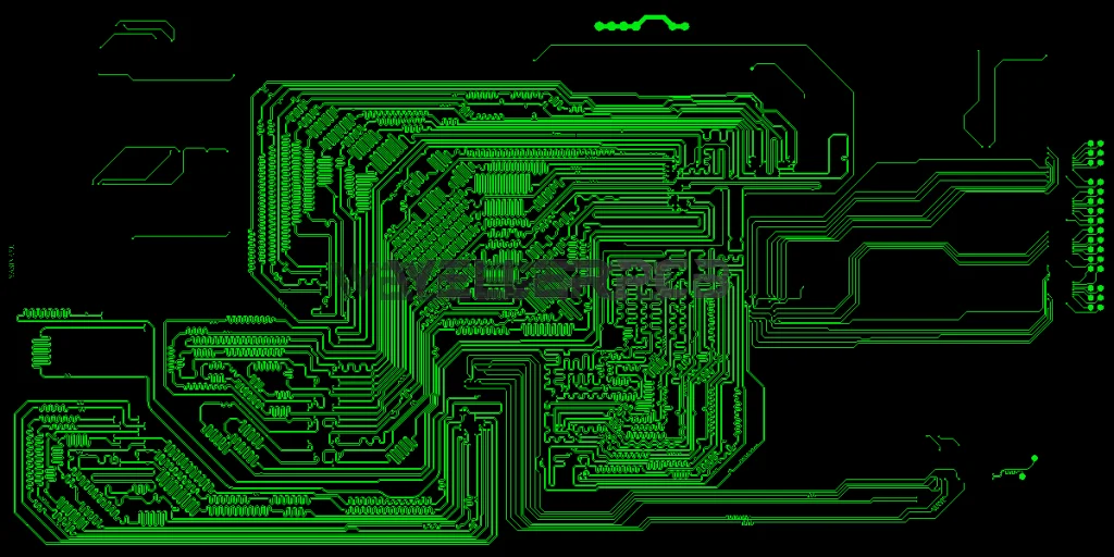
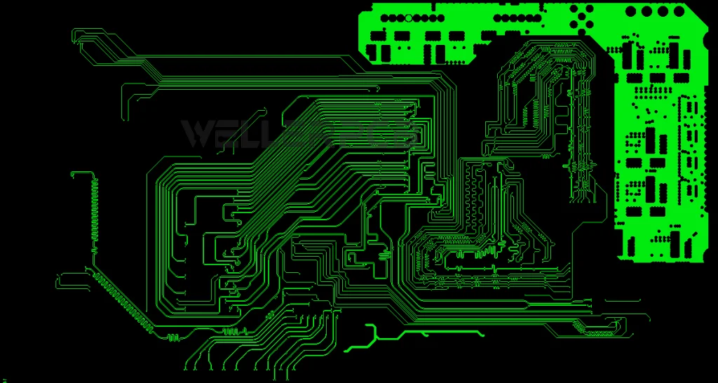
1. Signal Layers
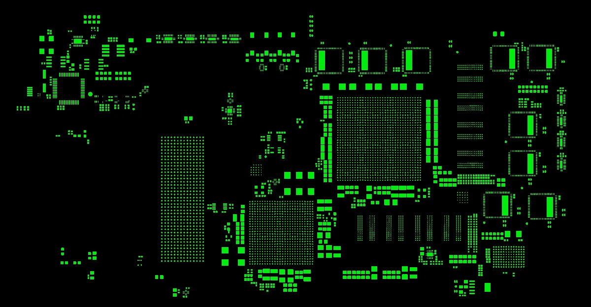
The signal layer is used to place copper traces that connect digital or analog signals. Altium Designer circuit board can hage 32 signal layers, of which TOP is the top layer, Mid1-30 isbthe middle layer and BOTTOM is the bottom layer. Traditionally, the Top layer is also called the component layer, and the Bottom layer is also called the welding layer. And the copper signal layer is the most important layer in a printed circuit board.
2. Power Plane Layers
The power layer is a circuit layer in the printed circuit board that is mainly used to connect the power supplies and ground path. It is designed to give your PCB a steady supply of voltage. The layers with power planes supply components with power through contact path with a via featuring a trace.
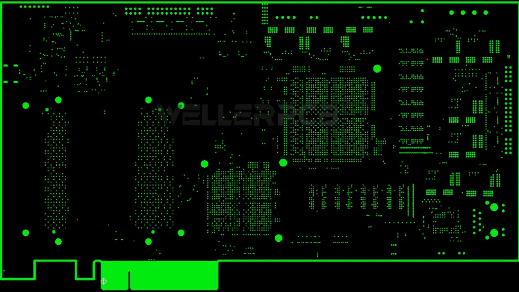
3. Ground Plane Layers
Typically,the ground plane on a printed circuit board is a circuit layer with large copper zone connected to circuit ground point. It is used as the return path for current from many different components. This zone of copper is sometimes only a small portion of the circuit board, or it maybe one entire board layer in some multi-layer PCB design. Eve it maybe occupy multiple layers, depending on the exact needs of the circuit design.
4. Soldermask Layer
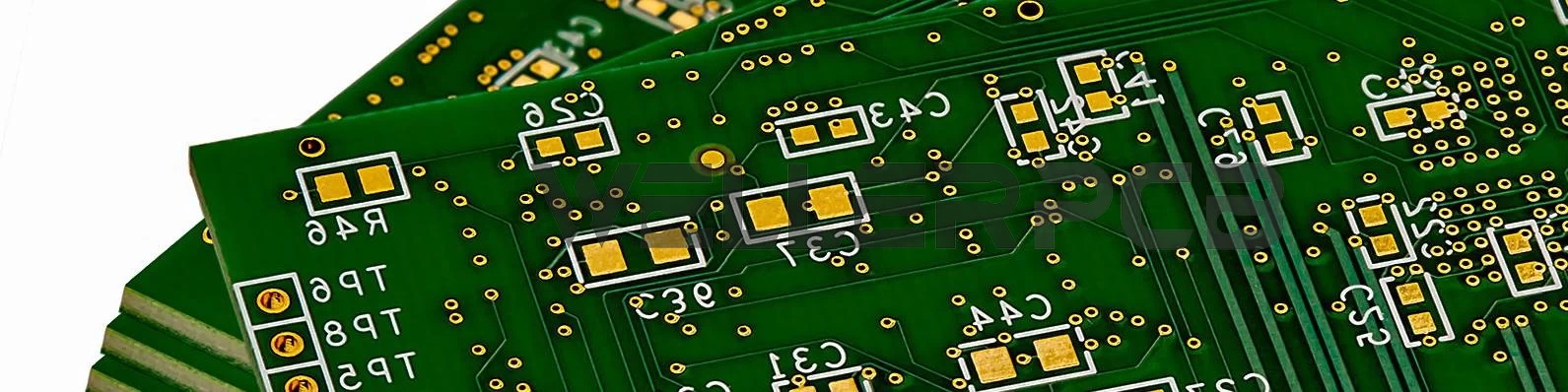
This layer is also a part of the PCB itself. Soldermask layer is on the copper layer. This layer makes the PCB look green, and it covers the traces on the copper layer thereby preventing traces on the PCB from direct contact with air (oxidation), contact with other metals, solder or other conductive objects and causing short circuits.
The existence of the Soldermask allows you to solder in the correct places and prevents solder bridges. We can see that the Soldermask covers most of the PCB (including the traces), but exposes the silver hole ring and the tin on the SMD pads for soldering.
Soldermask can be applied in various ways and its types are based on the application process. They include the epoxy liquid, the dryfilm photoimage amd the liquid photo image.
5. Pastemask Layer
This is also called the ‘Solder paste layer’. It has a similar function to the Soldermask, except that it represents the pad of the corresponding surface mount component during machine soldering. And it is not a part of PCB. Protel99 SE provides Top Paste (top layer) and Bottom Paste (bottom layer) two solder paste protection layers.
Mainly for SMD components on PCB boards. If the board is all placed with Dip (through-hole) components, this layer does not need to output the Gerber file. The pastemask is an essential material used in the production of pcb. Solder paste must be applied to each SMD pad before mounting SMD components to the PCB, this Pastemask file must be required for the stencil used for tin coating, so that the film can be processed.
The most important thing about the Gerber output of the Pastemask layer is that this layer is mainly for SMD components, and compare this layer with the Soldermask layer introduced above, find out the different roles of the two, because the two film pictures are very similar from the film picture.
6. Silkscreen Layer
The white characters are the silkscreen layer. Letters, numbers, symbols, logos, and components were printed on the silkscreen layer of the PCB, which can facilitate assembly and guide everyone to better understand the information, designs and unique numbers of the board.
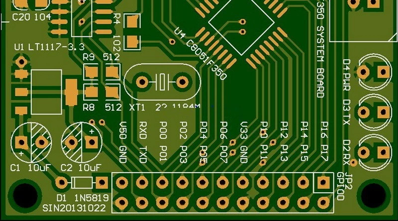
We often use silkscreen symbols to mark certain pins or LED functions, understand warning signs and symbols. It makes use of an epoxy ink or an acrylic ink (depending on the type of printing being used) instead of the common printing ink. The 3 major types of silkscreen printing are : manual screen printing, liquid photo imaging and direct-legend printing.
7. Mechanical Layer, Keep-out Layer
The mechanical layer defines the appearance of the entire PCB board. In fact, when we talk about the mechanical layer, it refers to the shape and structure of the entire PCB board.
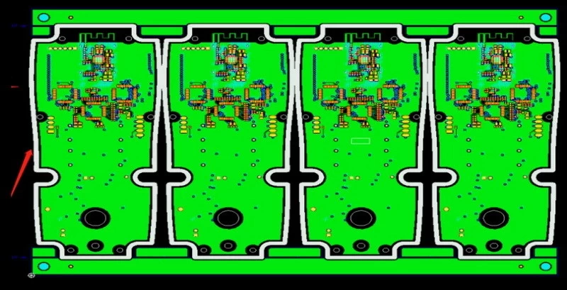
The keep-out layer is to define the boundary when we distribute the copper of electrical characteristics, that is to say, after we first define the keep-out layer, in the subsequent layout process, it is impossible for the track with electrical characteristics to exceed the boundary of the forbidden wiring layer.
8. Peel-off Layer (bottom)
A peel-off mask is applied to only one side of the PCB, which is mainly the bottom side. The mask is a form of protection during construction because of the high rate of their tear-resistance. The peel-off area in which the mask will be applied should be as big as possible on the PCB to make them easy during removal after PCB assembly.
9. Drill Layer
Whether your PCB is single-layered, double-layered or multi-layered, they all require Drilling. Drilling is basically the creation of holes or slots on the PCB before adding other parts/components.
It is the most expensive and time-consuming part of PCB construction. It is also the most complicated and delicate process which requires a lot of precision and accuracy. PCB drill holes have different classes which are based on their ability and inability to carry current.
Also, there are different hole types, and they include; tool holes, locating holes, via holes, mounting holes, etc.
hese holes require different types of drilling, but the major types are; mechanical and laser drilling.
Things to consider when drilling:
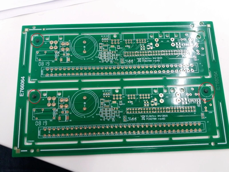
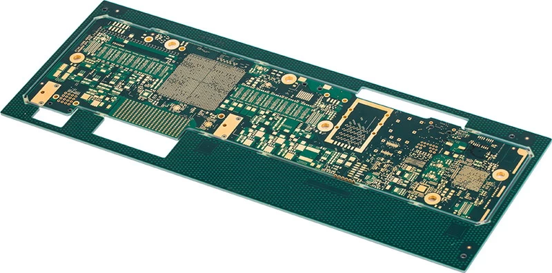
10. Rigid Printed Circuit Board
This is the most ancient and oldest form of PCB. It is very common and popular in the PCB world. Rigid PCB gives room for mass production which promotes effective decrease in it’s cost. It is built on a rigid-base layer that can not be twisted, bent or folded, which is due to how strong and durable it is compared to other types (this is why you cannot change or modify it after it has been manufactured).
They consist of different layers which are joined using either an epoxy or acrylic adhesive and heat. These layers include; copper layer, substrate layer, Soldermask layer and silkscreen layer. The Flex PCB and Rigid-flex PCB are both gotten from it.
Also, there are different hole types, and they include; tool holes, locating holes, via holes, mounting holes, etc.
hese holes require different types of drilling, but the major types are; mechanical and laser drilling.
Rigid PCB can be applied in the following industries;
11. Flex Printed Circuit Board
It is built on a flexible-base layer (e.g., polyimide) which gives it the ability to bend, twist and fold. It also aids the movement of electrical current and also connects electronic components for different devices. They are generally used in electronics, automotive, medical industry, manufacturing of sensory materials and robotic arms, also found in satellites and resistors.
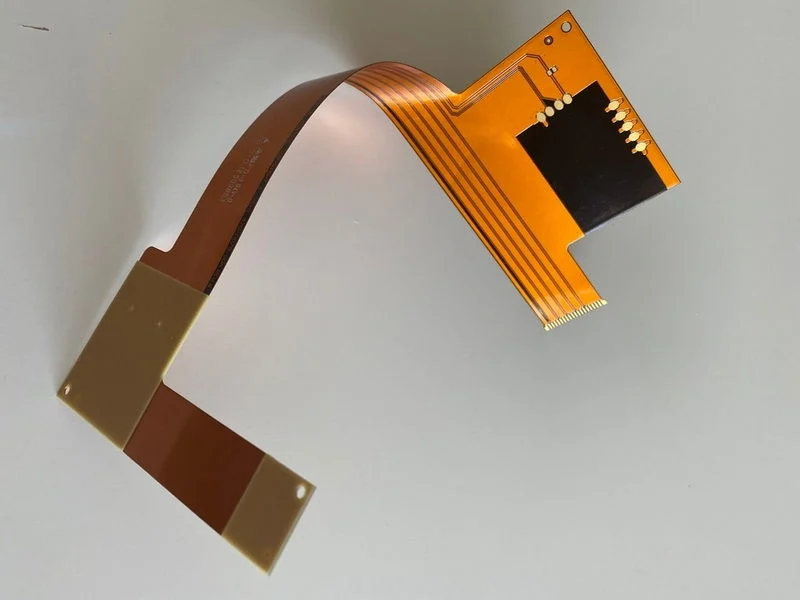
12. Rigid-flex Printed Circuit Board
This is a hybrid board that has the combination of both rigid and flex RCB features for effective and increased performance, also to enhance the reliability and flexibility of the PCB. The materials of the Rigid and Flex base layer are connected to each other.
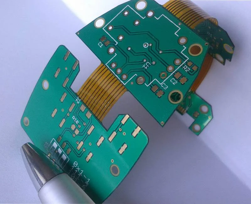
The rigid-flex PCBs are designed to be smaller and light weight to fit it into small devices which does not hinder its functionalities, but rather enhances its demand rate especially in the telecommunication industry. They also have the ability to handle more complex functions and has a high operating capacity.
The rigid-flex PCBs are designed to be smaller and light weight to fit it into small devices which does not hinder its functionalities, but rather enhances its demand rate especially in the telecommunication industry. They also have the ability to handle more complex functions and has a high operating capacity.
Conclusion
Before the introduction of PCB, there were other boards that were popularly used; the wire wrap and point-to-point construction. But ever since PCB has been able to solve more problems, production of circuits in larger amounts is faster and cheaper since all components can be put together in one operation, and they are used in almost all electronic products, those wiring methods are now rarely used.