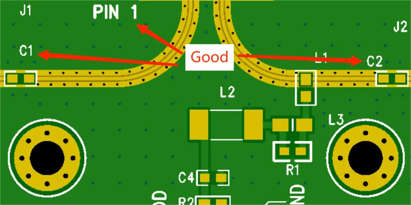
Silkscreen is one of important compositions to a complete PCB board fabrication, especially it’s high importance to finally circuit board assembly.

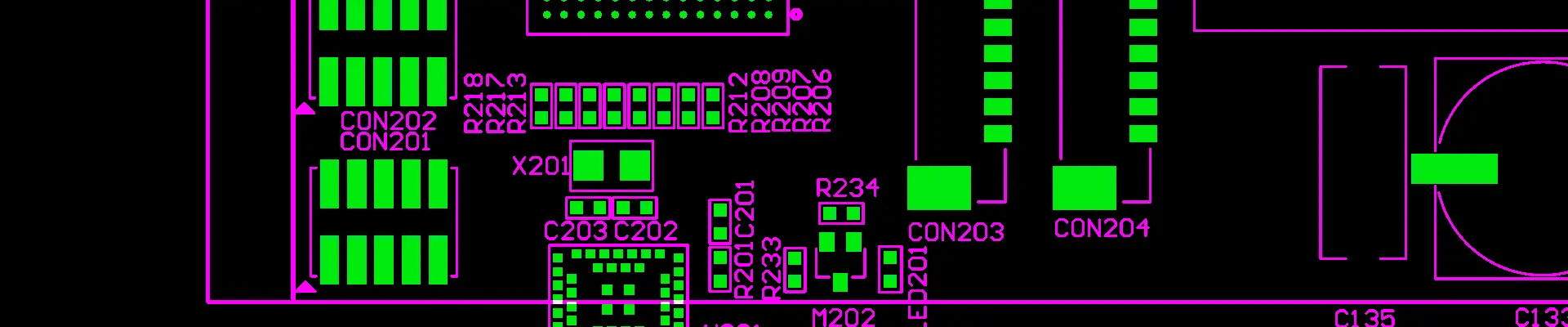
The silkscreen is a typical layer of chemical ink printed on the bare circuit board used to identify the electronic components, Rev. no.#, test points, marks, logos, symbols, etc.

2024/04/PCB-Silk-screen-review-in-Gerber.webp
PCB silkscreen review in Gerber
2024/04/The-silkscreen-identification-in-Complete-PCB.webp
Complete PCB with silkscreen printed

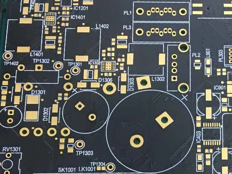
Normally it is printed on the components side or on the solder side, but any side is no matter and can be freely defined by PCB designer as long as it will be as a clear identification to reader as it’s purpose.

What Types of Colors that PCB Silkscreen Have?

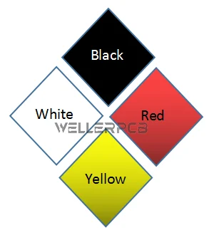
Normally, the white is a generic silkscreen color applied in most of printed circuit boards, which is a common color and friendly to manufacturing process. Meantime, other color such as yellow, red, black is widely used in initial of PCB board design and manufacturing. Pink silkscreen color is also a favorite color to PCB designer but we do not recommend to use this color due to it’s special characteristics with result that unfriendly to manufacturing process.

2024/04/The-Common-Colors-of-PCB-Silkscreen.webp

How It Comes Out By PCB Manufacturing Process?

Commonly there are two production ways to get printed circuit board silkscreen:

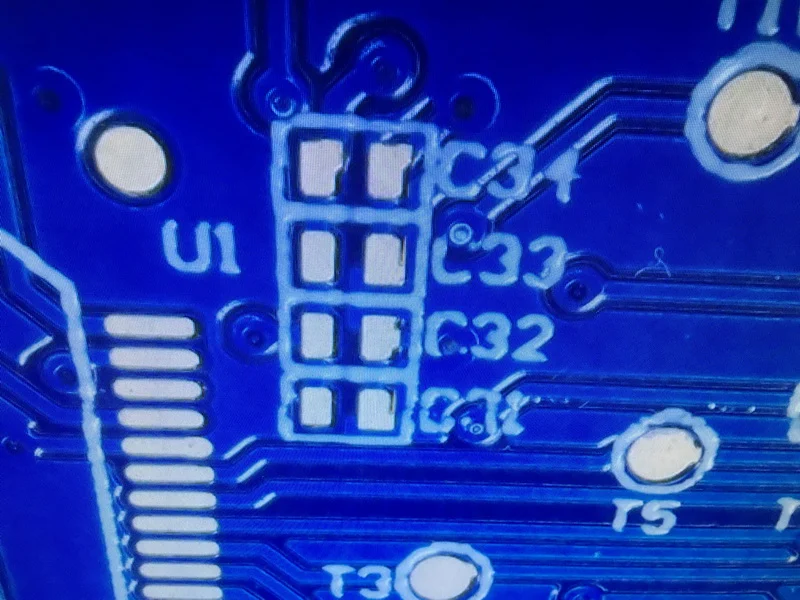
One method is done by PCB manufacturers via auto ink printing process as below which a little blurry on the edge of the PCB board. Which sometimes have blurry around the edge of the silkscreen letter.

2024/04/traditional-ink-print-PCB-silkcreen.webp
Traditional ink printing silkscreen
2024/04/Laser-printing-PCB-silkcreen.webp
Laser Printing Silkscreen

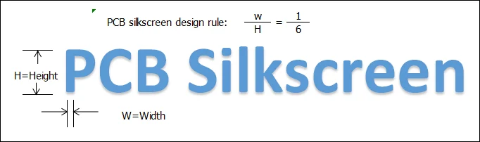
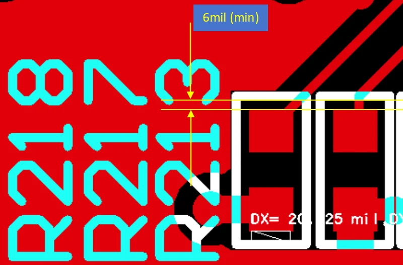
Basic Notes About PCB Silkscreen Design

When it comes to PCB layout in silkscreen stage, the design is better to follow this regular ratio that width/height=1:6, which can be sure the silkscreen presented on the complete PCB board at a high resolution performance.

2024/04/General-rule-for-PCB-silkscreen-design.webp

Note that the width of the silkscreen is changing from its different base copper thickness listed as in below table:

PCB silkscreen design guidelines

Base Copper(oz) Minimum Silkscreen width (mil) Silkscreen Height (mil)
0.5 4 24
1 5 30
2 6 36

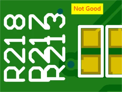
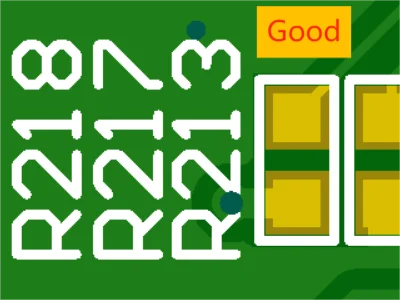
6 Key Points in PCB Silkscreen Design

Place and direction of the components: Generally, it would be better to mostly place all the components in the same direction instead of different directions, or else which will take several extra works to PCB assembly’s functional test, verification, soldering, etc.

2024/04/PCB-Silkscreen-direction-guidelines.webp

Dot not place the silkscreen on the through plated holes.

2024/04/Bad-PCB-silkscreen-on-the-through-plated-holes.webp

Do not place the silkscreen over on the RF track (Radio Frequency)

2024/04/Bad-pcb-silkscreen-placed-on-the-RF-track.webp
2024/04/Good-pcb-silkscreen-on-the-RF-track.webp

The direction of the silkscreen should be the same as the orientation indicated in the data sheet of the components (For example, IC, diode, Led, etc). This will avoid the misunderstanding to PCB assembly process.

For multi-pin components, which have sequential no.# of pins, the pin no.# 1,2.3…. should be presented on the silkscreen.

2024/04/The-polarity-of-capacitor-EEE-FT1H331AP.webp
down-arrow
2024/04/The-polarity-design-of-capacitor-EEE-FT1H331AP.webp

The silkscreen profile for some special package components (BGA, QFN, etc) should be the same size as it’s component profile.

2024/04/The-PCB-silkscreen-design-for-outline-of-ICs.webp

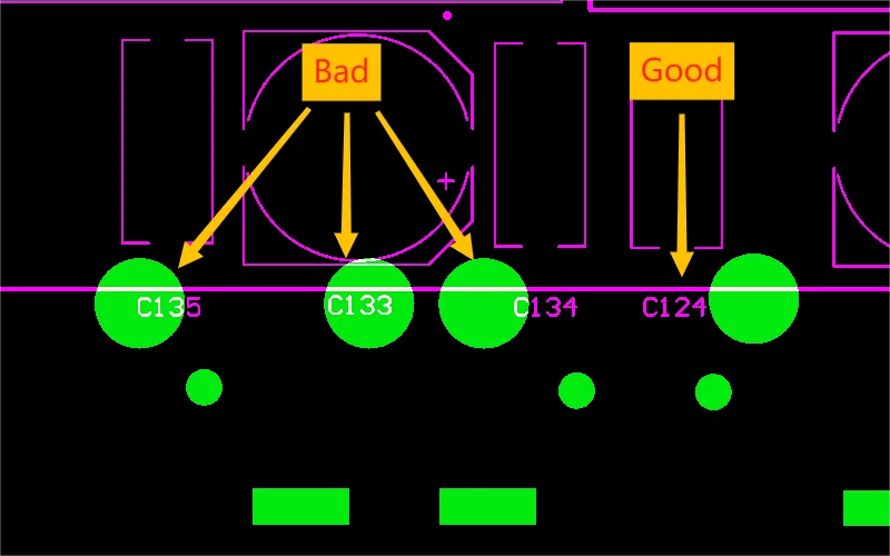
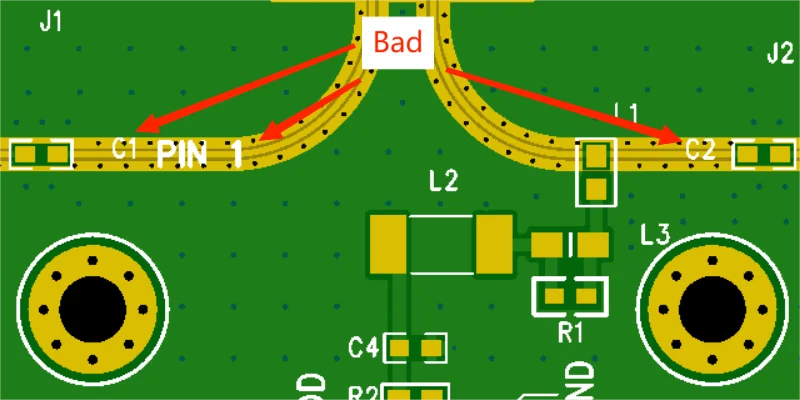
General Guideline to PCB Silkscreen Design

Width: the silkscreen width≥4mil, (the silkscreen would not be able to be printed out if it’s width less than 4mil).

PCB silkscreen design guidelines

Base Copper(oz) Minimum Silkscreen width (mil) Silkscreen Height (mil)
0.5 4 24
1 5 30
2 6 36

Spacing: the silkscreen should have 6mil spacing to solder mask opening pad, component soldering holes, test points, fiducial marks, etc. It will be as an anti-solder resistance once the silkscreen overlapped on the SMT PADs.

2024/04/The-PCB-silkscreen-design-guidelines-soldermask-opeing-PADs.webp

Silkscreen do not overlap each other.

It must be presented as sequential turns (from left to right; from top to bottom)

Each silkscreen designation should be matched with it’s component accordingly (do not confuse the reader)

For some specific polarity or orientation components, the polarity point or the Pin 1 should be clearly and correctly marked.

Some extra marks or signs can be moved to GM layer (Geometry).

If the PCB boards have a limited spacing to put the silkscreen, the silkscreen layer can be canceled in PCB fabrication process, but it must be present by another layer as assembly drawing (Top or bottom layer).

The bottom silkscreen layer must be viewed in Gerber file as mirror format.

If you have other concerning about PCB silkscreen before your circuit board design process, please freely contact us via service@wellerpcb.com.