What is Back Drilling or Controlled Depth Drilling in PCB?
PCB Back Drilling is one of the special controlled depth drilling (NPTH) in the loop of PCB manufacturing process. Normally, there will be various challenges in engineering and production when it comes to PCB design and printed circuit board manufacturing and one of them is how to ensure high performance of retaining signal integrity.
When the electric PCB board transmits a signal, the signal quality received will be subjected to distortion from signal noise, crosstalk effect, and other undesired effects.
Thus, necessary incorporating design and manufacturing practices must be involved in to limit such effects and increases signal integrity. Via holes stubs often plays an important role to contribute to a decrease in signal integrity which can be effectively resolved through the use of via holes drilled by the back drilling process.
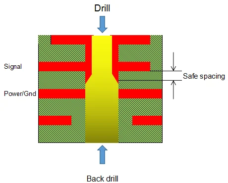
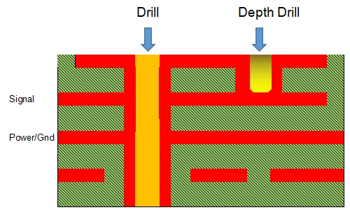
Back drilling (or called Controlled Depth Drilling (CDD)) is a technique calling which is used to remove the partial unused copper barrel from a through-plated-hole (via) in a electronic PCB board.
As these type of holes are back drilled to a certain-controlled depth, so this type of drilling process is also called PCB controlled depth drilling. In the back drilling process: the controlled depth tolerance is a critical parameter to limit the drilling’s depth, to make sure that the drilling not to hurt the useful copper which should be used as the conductive purpose to other layers.
So the back drilling technology can’t remove the via stub completely but necessarily keep useful cooper barrel as it is.Usually, it will residue a little (stub length smaller than 10mil).
What kind of PCB need to be drilled by back drilling?
Usually, the PCB board holes are drilled as through holes (from top to bottom), when the trace which connected the via holes are close to top layer (or bottom layer), will produce stub bifurcation at the via hole of the PCB interconnection link, it causes signal reflections and affects signal quality. This effect has a greater impact on higher-speed signals.
General understanding,the circuit track on the PCB board with it’s Signals with a rate of ≥1Gbps need to be considered to add back-drill design to get a high quality of signal transimission. Of course, the design of high-speed interconnection links is not so simple but a system engineering. If the chip’s drive capability is strongly enough, or the system interconnection links are not so long, maybe the signal quality can pass perfectly without any back-drill design. Therefore, the most reliable way to determine whether Back-drill needed or not is through system interconnection link simulation.
Except back drilling technology, you can realize that alternative construction techniques could also be used to minimize or optimize the stub length. These include laser-drilled vias (microvias) holes, or blind and buried vias, and alternative stack-up arrangements – where circuit track traces are moved to layers closer to the end of the via stub. Also, back-drilling is not necessary for high frequency (greater than 3GHz) boards since alternative strategies are used to reduce signal reflection.
However, to reduce the signal loss in many high-density PCBs or backplanes/mid-planes, these options in above are not always convenient from both manufacturing facility and cost standpoints. Thus, the only viable option is to remove the via stub by back drilling. Back drilling is very necessary for high frequency (greater than 1GHz within 3GHz) boards when blind vias holes are not viable.
And due to many layer counts with the PCB, some holes are not suit to design as blind holes,(for example, the 16L PCB, some via hole need to connect with L1-10 also another via holes need to connect with L7-16, this design holes is not suit for blind holes but suit to design as back drill)

Back-drilling Process Flow in the PCB Manufacturing Process
Back-drilling PCB Design Notes and Common Problems
It is needed to separately output back-drill layers to the PCB board manufacturer, together with the specification which layer to which layer need to the corresponding back-drilling. The back drilling hole size need to be bigger than first drill holes 0.2mm at least, the back drilling through layer need to ensure hole to trace 0.35mm for first drilling (0.2mm for back drilling).
When design PCB stack-up, should consider the dielectric thickness to avoid the trace to be drilled by the back-drilling. If need to drill to “M” layer, the dielectric thickness(distance) between the close to layer which no need to drill and the M layer should be at least 0.2mm.
If you need to understand more about “back drilling and depth drilling”, please contact us by service@wellerpcb.com, and our engineer will be happy to answer your any questions.