
Top 12 Considerations to Know Before PCB Layout
High quality of PCB design and layout will take much convenience to PCB fabrication & manufacturing process, and improve the reliability of the SMT assembly process.
These guidelines shown here are focused on a few key points that will help you with routing, manufacturability, basic signal integrity, and PCB assembly.
1. The spacing size between SMD components
Enough spacing between SMD components is the first important thing that PCB layout engineer need to take care. Too small spacing would raise up the difficulty of solder pasting and take soldering joints between soldering PAD. Below is some proposed spacing for designer’s reference.
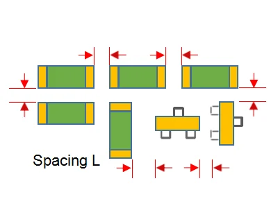
Spacing for SMD components:
Homogeneous SMD components: ≥0.3mm
Heterogeneous SMD components: ≥0.13*H+0.3mm (H for maximum height difference of neighboring components)
Spacing for hand-soldering components: ≥1.5mm
Above spacing is reference to PCB designer for layout work from WELLER, different PCB assembly house have different SMT capabilities.
2. The spacing size between SMD and Through hole components
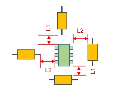
Homogeneous SMD components: ≥0.3mm
Refer above picture illustration; enough spacing should be placed between DIP and SMT components, proposed spacing is 1-3mm. Today, less and less though-hole components applied into electronic devices design due to it’s complicated soldering process and expensive cost.
3. The placement of IC’s decoupling capacitors
A decoupling capacitor (also called bypass capacitor) is a capacitor used to filter high-frequency noise in power supply signals.
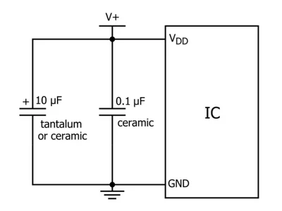
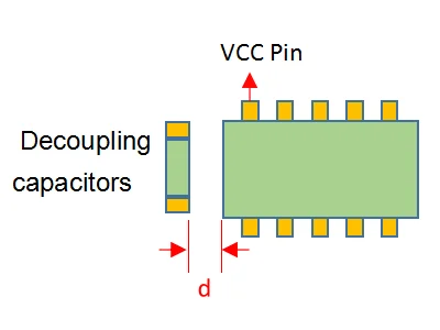
Proposal: Decoupling capacitor placed as close as possible to an integrated circuit (IC) on a PCB layout. Each power supply port need to match one decoupling capacitor if multi power supply ports exists to IC.
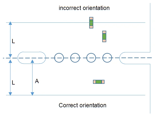
4. The importance of orientation and spacing of the components close to boarder.
Commonly, PCB panelization is preferred both by PCB fabrication house and PCB assembler. As PCB manufactured by panel can optimize the raw material utilization to reduce the manufacturing cost; also, it can improve Contract Manufacturer (CM) efficiency at the SMT assembly process.
Two basic premises in layout must be met for PCB panel:
4-1. The components neighboring to the PCB boarder must be parallel with board outline( this will lead components to afford uniform mechanical stress from de-panelizing; for example, the components at the left aside in above picture could be dropped off it’s soldered PAD from the process of de-panelizing due to withstanding the Non-Uniform mechanical stress.
4-2. Do not place the component at the zone close to the PCB boarder(avoid damaging components when de-panelizing working panel).
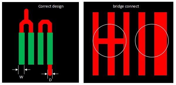
5. Optimizing the continuous connecting PAD.
If some serial SMD PADs need to be connected each other, design them by Serpentine Routing instead of direct bridge connection. And the width of the track need to be cared.
6. Heat (thermal) Dissipation to the PAD on the certain regions must be cared.
Obviously, better heat (thermal) dissipation, better working performance of the electronic devices. So, the designer must take high care to how to design and layout PCBs to prevent heat from accumulating in certain regions, which over time lead to serious failures, perhaps even causing could catch fire. Even if nobody is hurt, that boring heat can affect performance and damage the components. Therefore, it is very necessary to take care Heat (thermal) Dissipation to the thermal PAD when do PCB design or layout.
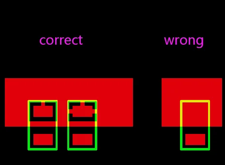
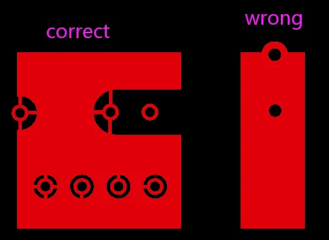
If the PADs locate in the common region, the right solution at above picture is the better option, chose 1 track or 4 tracks pending on the currency volume. If using the left solution at above picture, it could cause some difficulty in repairing or disassemble the components, as the temperature of dis-soldering could be dissipated by the large copper ground and lead to the hardness of dis-soldering.

7. PCB teardrops design in your PCB layout
A teardrops are extra copper with some certain shapes used in a PCB layout is to provide extra strength so that the vias can be enough strong to withstand thermal and mechanical stress. Especially the regions at the junction of a pad or via and a trace line, or when a trace routing between wide and narrow. For example, if part of your trace line width is changing from 10 mils to 4 mils, then the teardrop is necessarily to be added at the transition point to reduce any potential stress or hairline cracks.
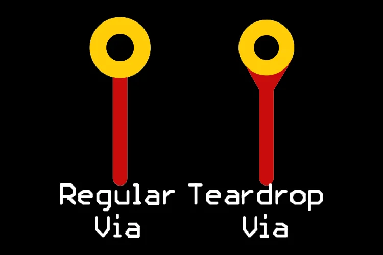

The advantages of teardrops
7-1. Avoid the reflected signals from sudden narrowed transition trace line, keep the smooth and steady between junction connecting between trace and PAD.
7-2. Avoid the hairlines and cracks from impact stress between PAD and trace.
7-3. Facilitate in etch process in PCB manufacturing.
8. Consistent trace width between soldering PAD
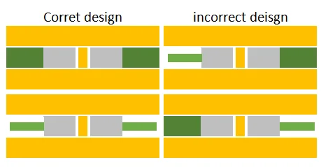
The each trace connected to the PAD should have the same width of size
9. Leave unused PAD and connect them to electrical ground
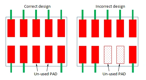
The un-used PAD should be kept at there, and correctly connect them to Electrical Ground.
For example, two pins of the IC chips on above picture are non-functional pad, but they are existing on the IC chips. It could cause signals interference if no connection to electrical ground.
10. Avoid the via holes on the solder PAD.
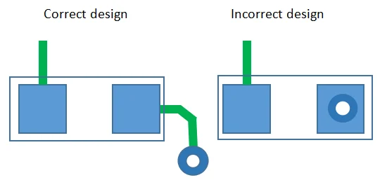
If it is no choice, it is better not to put your via holes on the soldering PAD, this will cause soldering problem due the leaking solder from the hole; or else, PCB manufacturer have to use VIA IN PAD technology to avoid this problem but manufacturing cost raise up and lead time would be longer.
11. Enough spacing between trace or components and PCB boarder
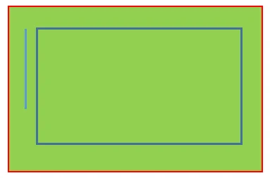
Keep the spacing as large as possible between the track or components to the PCB boarder. Especially for single layer PCB which most large paper base material, the components or track closely placed to the boarder would be impacted from mechanical stress.
12. Electrolytic capacitor placed as far as possible to some possible heat source
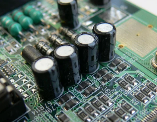
Firstly, to verify whether the electrolytic capacitor match the working temperature of the electronic devices, secondly, keep electrolytic capacitor as far as possible from heating source, to avoid it’s internal electrolytic liquid be dry from impacting of the heating sources.
Above considerations is the basic notes that should be paid attention to, these cover most issues in PCB assembly process. If you have other special components or PCB layout issues, please contact us freely.


