When you are place and PCBA order to WELLER, you are buying quality that pays for itself over time.

Our team will double review the terms and specification presented or related in your purchase order, or any any documents along with the order. This is to make sure your product specifications and quality controls are thoroughly understood by us, and to ensure that the product delivers what it promises.
WELLER will not change any specification unless get official approval from customer. This action are far more stringent than those of other suppliers.
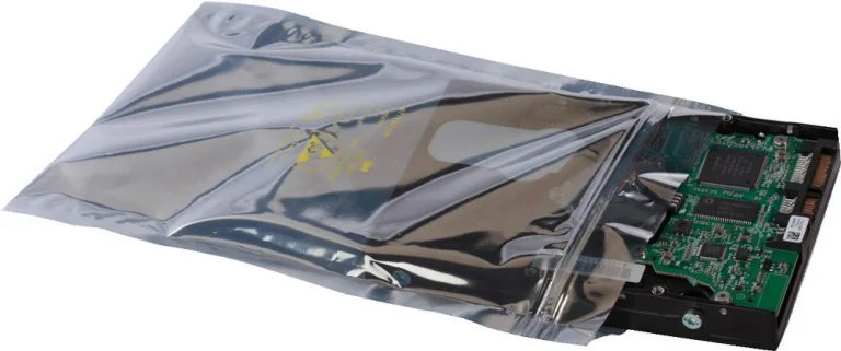
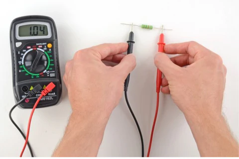
IMQC (Incoming Material Quality Check), this is to use necessary instruments and test equipment to have a global inspection to incoming material (components, bard PCB board, stencil tooling, etc), to make sure each material match the specification.
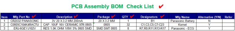
WELLER’s value: we always perform the BOM check list to make sure that the incoming component materials 100% conform it’s specification in the BOM, and the size match it’s pattern on the PCB board.
All the components must be original parts as customer specified, no any alternatives allowed without customer’s official approval.
This is a premise but core work to make sure the production moved forward correctly.
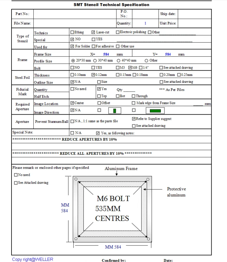
It is a tooled aluminum foil (or stainless steel foil) with opening window cut by laser, to simply transfer the solder paste via this window to the surface of SMD pad on the bare circuit board.
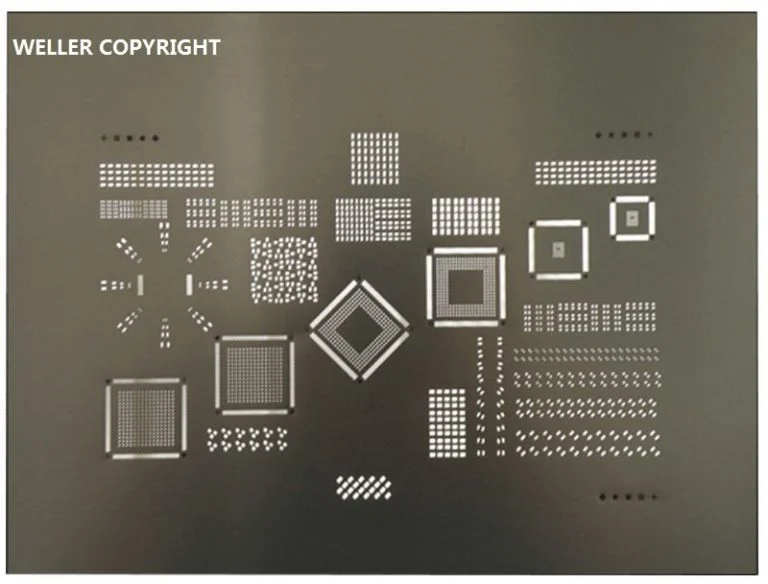
The quality of the stencil is most critical to the final PCB assembly’s quality, all WELLER’s stencil is tooled by high quality of aluminum material with high precious laser cut process with REDUCE ALL APERTURES BY 10%.
Refer WELLER-SMT-Stencil-Technical-Specification
It is to load all the purchased SMD components by roll or tape into the feeders of SMT machine, the feeder location must conform to the components in pick and place file.
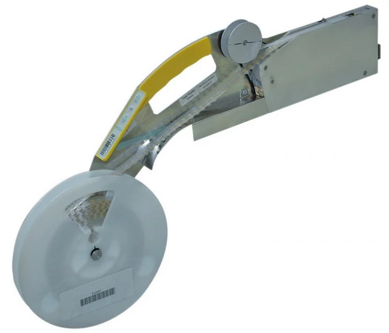
Feeder Setup
Reflow soldering profile
It is to transfer bare PCB board to the assembly process automatically.
All the bare PCB board load machine in WELLER is automatically controlled rather than manual transferring work done in other supplier. And, this directly lead to the production efficiency and capacity improved.
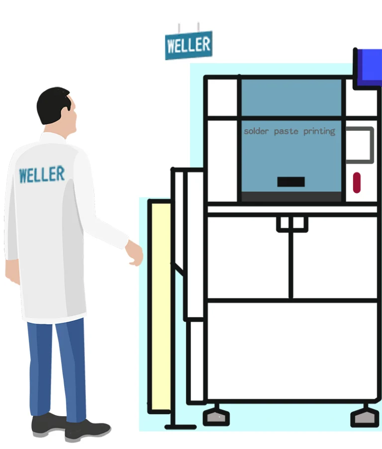
Solder paste printing is a core step in the SMT (Surface Mount Technology) assembly process.
It is to print the solder paste via stencil on the every one of the pads on the PCB board which need to be components soldered on. This work normally done by high quality solder printing machine or by manual work.
The two key points on this process is paste print machine and the material of solder paste.
In WELLER, All the soldering printing work is done by automatic machine which have high-accuracy positioning and high-speed printing and highly stable quality than other suppliers who do this by manual work to avoid affording the high cost of buying Auto-printing machines.
And, all the solder paste we used is ALPHA-OM-340, which have a most stable quality than other brand solder paste. And can apply to different end application of products (industrial PCB assembly, communication PCB assembly, medical PCB assembly, high density BGA or QFN PCB assembly, etc)
SPI means Solder Paste Inspection in PCB assembly industry. It’s work purpose is to check the solder paste deposits on the SMD component pads of bare printed circuit boards (PCBs) before loading the components on it. This is to sort out the potential flaws from solder paste printing process before form a SMT assembly.
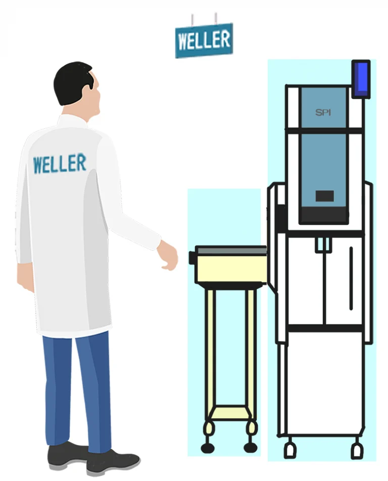
All the assembly lines in WELLER is matched with SPI machine, this is much more safe and high quality rather than most other suppliers who do not use any SPI or just make solder paste inspection by eyes.
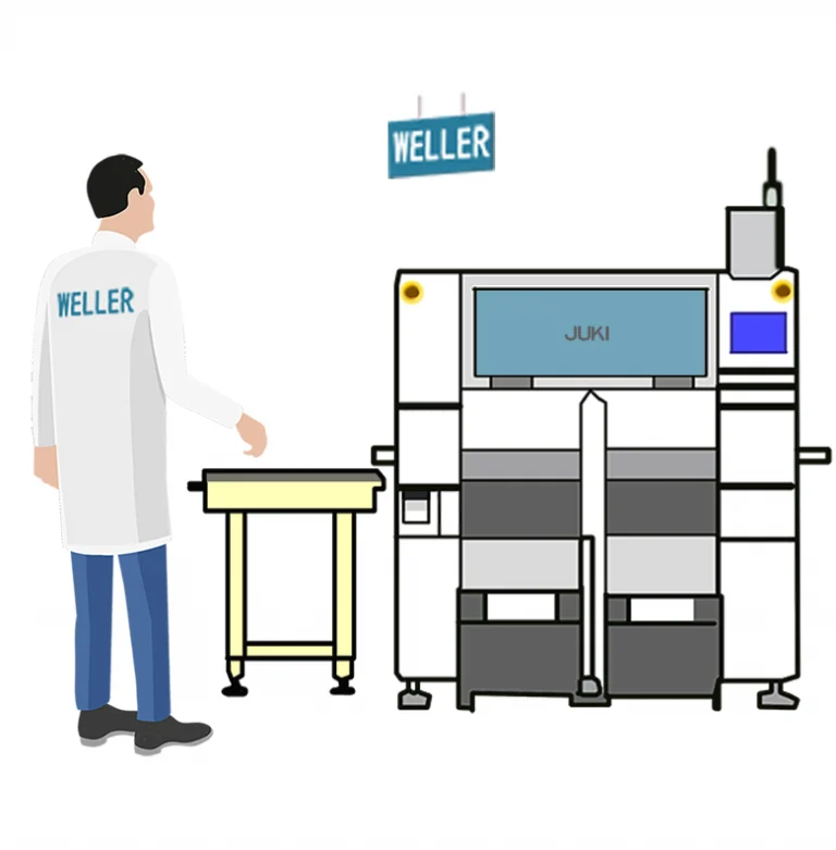
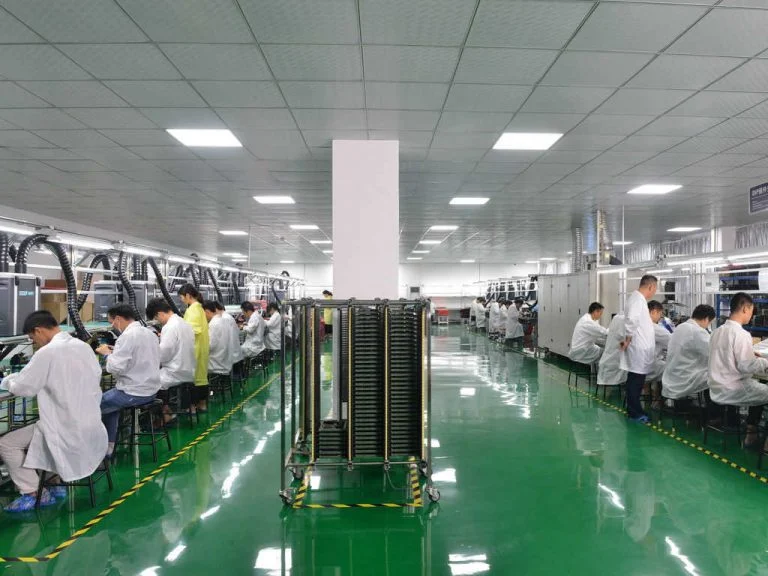
SMT (surface mounted technology) assembly is one of important part of PCB assemblies process.
It is to mount the electrical components (surface mounted device) onto the PAD surface of a bare printed circuit board.
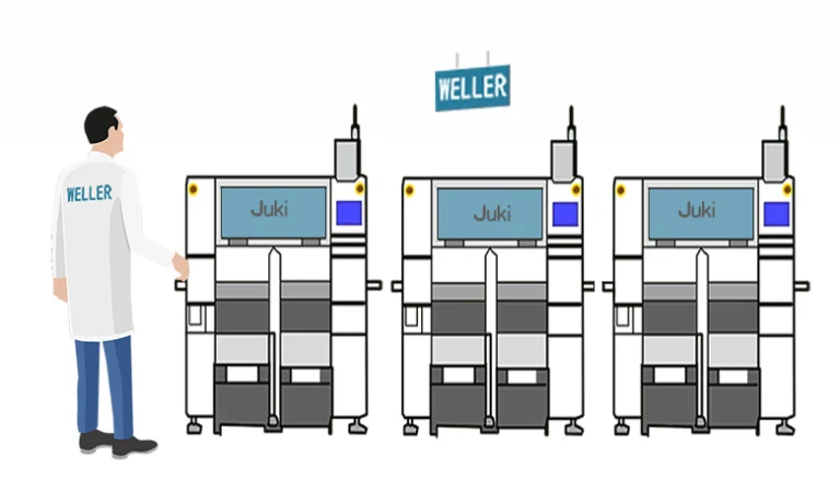
In WELLER, all the SMT machines in production line is from Yamaha with it’s latest model to ensure high accurate and high efficiency production work. No need to subcontract work to outsource which other supplier do.
Universal SMT assembly which is a supplement to the regular assembly.
This is to assemble some in-regular shape size of components by unique assemble machine.
The production efficiency can be highly improved by this universal assembly optimizing process.
Reflow soldering is an important part of assembly process by which the molten state solder paste will turn to the permanent solder joints. So as that the SMD components is soldered on the SMT pad of the bare printed circuit board.
After this process, the components has been fully soldering jointed with it’s SMT pad under them.
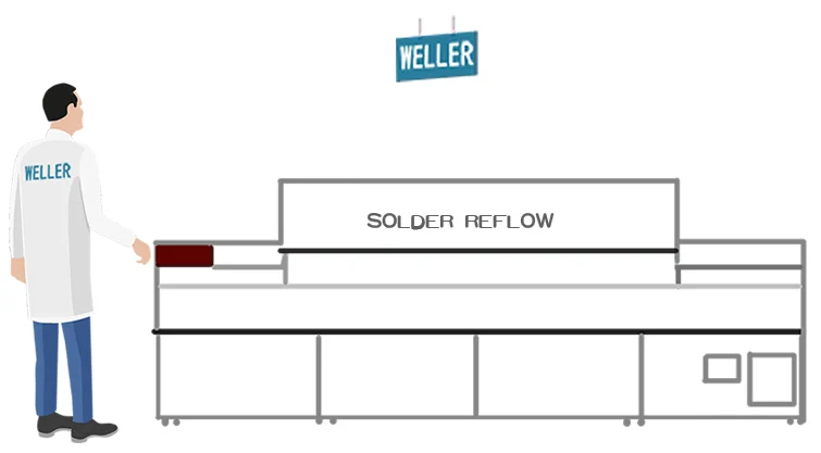
Reflow soldering machine
In Weller, we are using latest 12 temperature zones solder reflow machine to ensure the high quality soldering performance, especially for some fine pith and high density BGA components. And, all assembly production record of soldering profile is kept 1 month at least for available traceability unless spherical request from customer. Which is better than other suppliers who do not have any production record backup.
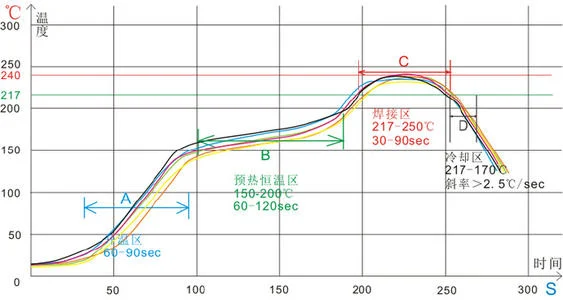
Reflow soldering profile
AOI (Automated optical inspection) is an important step of inspection in circuit board assembly process. It is an automated visual inspection of PCB(printed circuit board) assembly where a camera autonomously scans the SMD components under test for both catastrophic failure (e.g. missing component) and quality defects (e.g. fillet size or shape or component skew). This is a critical inspections process to ensure good quality of PCB assemblies.
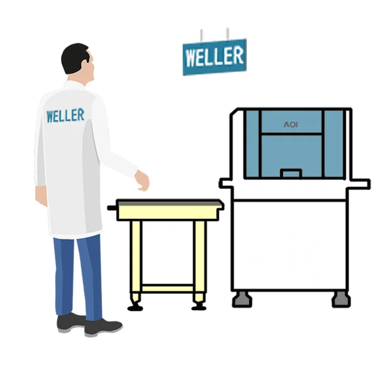
In Weller, all the assembly production lines is equipped by AOI machine. All the PCB assembly production (even each prototypes) is implemented AOI inspection, rather than other suppliers who use manual power (by eyes) to have a visual inspection to the board.
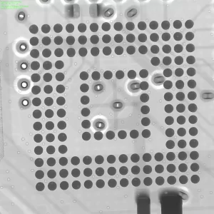
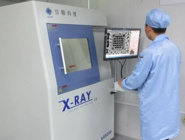 In WELLER, all the assembly soldering on BGA components, fine pitch components and QFN components must be done under X ray inspection with the machine equipped at our own house, and all the inspection records is backup in our system available for traceability. Rather than other suppliers who do not have x-ray inspection machine and have to subcontracted it to outsource or do not do X-ray inspection at all and pass the defects or failures the customers.
PCB DIP assembly is also called through hole components soldering process, it is to assemble though hole components by peak wave soldering process or by manual soldering work.
So this will be the time saved and quality controlled rather than the other supplier who subcontracted this process to outsources.
Functional test is to power on the assembled PCB board with firmware programmed in.
This is to dig out some hidden problem which escaped from the inspection in AOI and X-ray. This is best-safe option to make sure customer to receive the ordered PCB assemblies at correct quality.
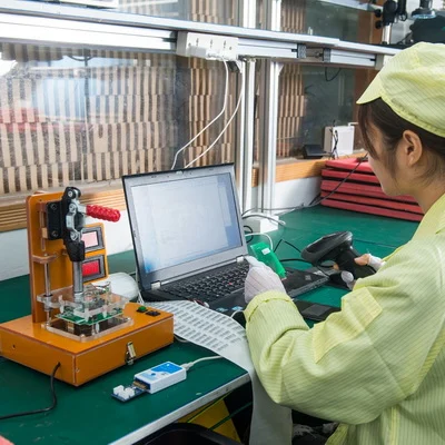
In WELLER, commonly we suggest customer to accept our request to firmware burning-in and power on their boards to implement a basic electrical function test, and do repair once some defects found at our house accordingly. So as that all the problem can be killed at our own house and not let them go to customer. Rather than other supplier who do not do any recommendation of functional test and the projects sometimes catch file when customer power on their boards after receipt.