Coplanar Waveguide Design for RF PCB
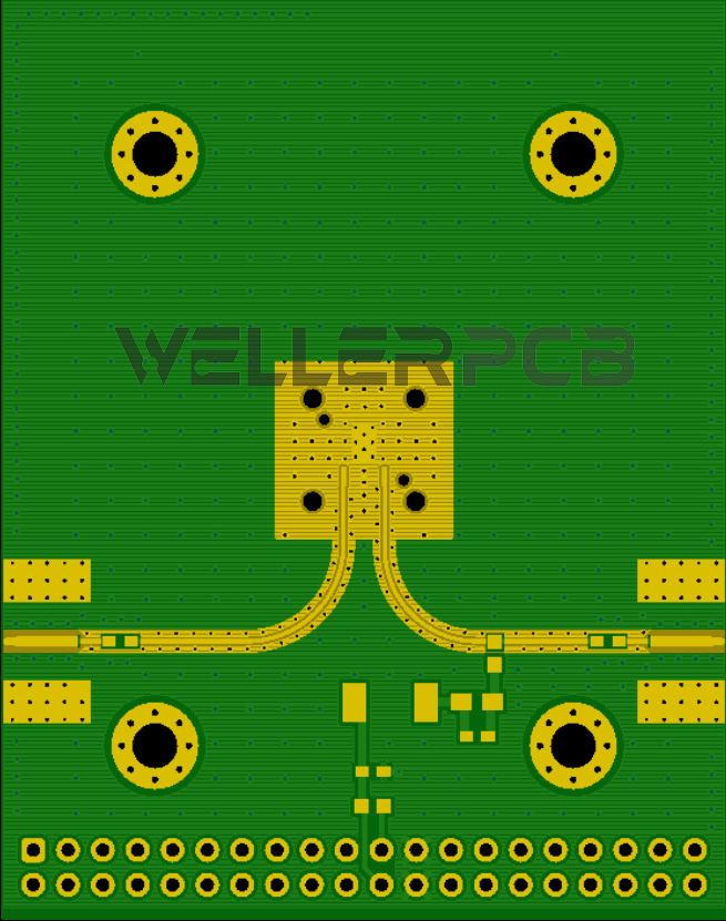
The printed circuit board with application in the RF (radio frequency) or high frequency such as radar system, Wi-Fi, Bluetooth, wireless system, high frequency analog system, etc., all of these type of applications need to include measures to ensure signal integrity. It would be very difficult to many high frequency systems with micortrip or embedded microstrip routing on the surface copper layer. However, coplanar waveguide routing is an ideal solution and widely used to solve the signal integrity headaches.

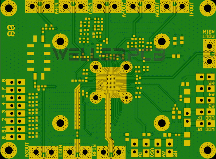
Most PCB design software (such as Altium) can be used to define the coplanar waveguide layout with a ground pour feature printed circuit board. This will be easily for PCB designer to define a coplanar waveguide on the printed circuit board. But a frequently asked question: when should the circuit board designer use coplanar waveguide layout (routing)? Here’s everything you need to know that before starting a design PCB with coplanar waveguide track in.
What is Coplanar Waveguide Routing?
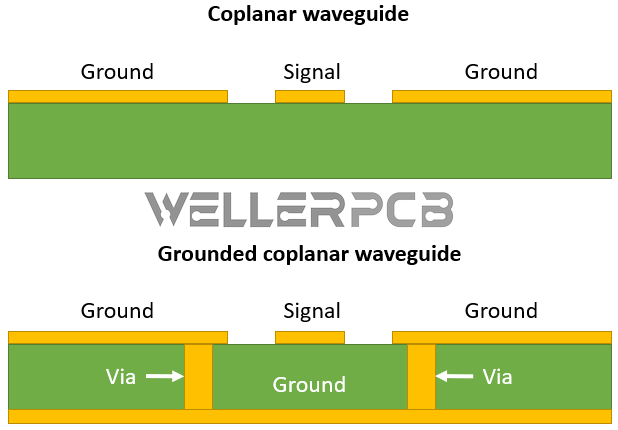
A coplanar waveguide is a simple routing style where a signal trace is routed on the surface layer and surrounded by ground pour on each side. The role of the ground pour on each side of a signal trace is to provide natural shielding for the signal against interference from other traces on a circuit board. Additionally, a ground panel layer is needed to be routed below this signal trace to provide high isolation in the PCB layout, this is shown in the image below.


How to Rout Coplanar Waveguide in an Exact Printed Circuit Board
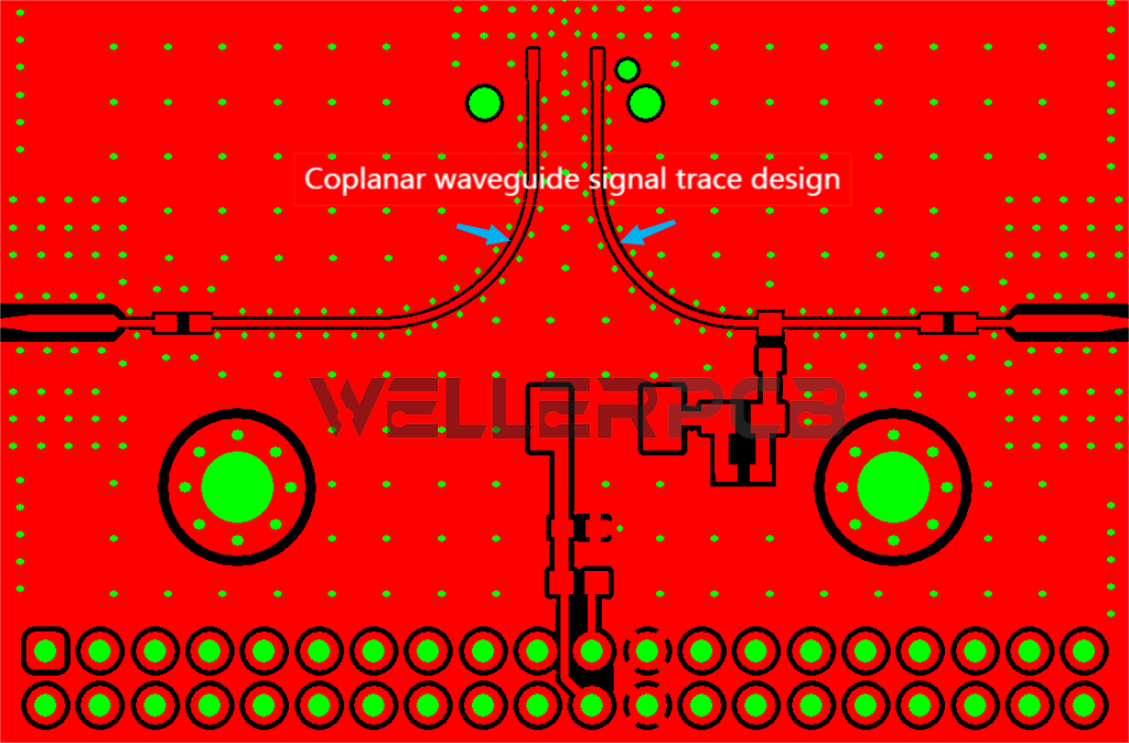
Below is the exact printed circuit board layout in Altium tool:
| 1. First step: refer below red layer, routing the signal layer with coplanar waveguide trace surrounded by ground pour on each side. |
| 2. Second step: refer below green layer: routing the grounded coplanar waveguide layer with isolated grounded plane |


Advantages of Coplanar Waveguide Routing
Compared to traditional design of microstrip and stripline traces, Coplanar Waveguide Design that placing a signal trace on the top layer with the ground pour track on each side of the signal trace has the advantage of causing a signal to see lower radiation losses. This type of Coplanar Waveguide Design also can reduce losses of the resistive heating because the signal thoroughly hugs the side of the circuit trace, instead of hugging the bottom of the circuit trace close to the rough interface with the substrate. Therefore, this means the signal will be much stronger at the receiver end of the circuit trace, and the shape of signals will not be distorted as they transfer along the trace.
Most circuit board feedtraces, applied in such as Wi-Fi transceivers , Bluetooth and antennas, require series and/or shunt components for impedance matching. As coplanar waveguides have a ground pour directly next the each side of the trace, so as these paralleled components can be directly mounted between the circuit track and the ground pour without adding extra routing though a via hole.
Disadvantages of Coplanar Waveguide Routing
Because coplanar waveguides design require the use of copper ground pour surrounding the circuit trace, therefore more or less the designer would have less utilization available on the surface layer. And the cost of all that copper on the surface layer will result in raising up the entire PCB board cost. Maybe you need a relatively thick substrate and a specific stack up, so you should keep the PCB layer count as low as possible if you are using a standard printed circuit board thickness.
There are closed-form waveguide equations for the impedance of a coplanar waveguide, but these formulas require to evaluate elliptical integrals. If you are more focusing on the design itself rather than the math, probably you do not have time to go and calculate the answers to these equations.One thing you will realize is that the signal trace impedance is extremely more sensitive to the spacing between the signal trace and the ground pour than it is to the cross-sectional geometry of the signal circuit trace.
It means that the designer needs to use as specific calculator which can numerically calculate the impedance of the signal trace. Fortunately that a lot of available calculators online can be used for specific coplanar waveguide geometries, including even a grounded coplanar waveguide. If you are using Alitum tool for your PCB design, you can find coplanar waveguide calculator at your software. Also, there is a great calculator from Sourcefourge that available for you to consider everything from your substrate dielectric properties and the frequency that you will work with in your printed circuit board.
Another potential issue is the surface treatment that plated on the surface of coplanar waveguides trace. Normally, the plating used on the copper surface is to prevent the trace from corrosion. ENIG (electroless nickel immersion gold) finishing has higher insertion loss on a coplanar waveguide compared that on a micro-strip. Other alternative surface finishing, such as HASL (hot air solder leveling), indeed has lower insertion loss but will have a rougher surface, leading to more losses in traces. Unless your design will operate at near to 100GHz, either surface coating will not be a problem to your application, as long as the lengths of your coplanar waveguides trace are not too long.

When to Use Coplanar Waveguide Design
As it’s excellent performance of high frequency signal transmission at lower loss, more and more designers are using Coplanar waveguide trace routing their high frequency printed circuit board, such as radar system, automotive, and UAV projects. The global price for components on these devices has been down recently, and it is possible to consider your projects with coplanar waveguide routing.
Typically, no specific frequency limit at that you should change your design from microstrip to coplanar waveguide layout and routing. But, coplanar waveguide routing is commonly used in industry types that operate at 10s of GHz, and in systems that require ultra-precise signal integrity. If you are designing a project with it’s frequency above 5GHz, then it would be worth to consider using coplanar waveguides on your most sensitive analog signals so as to purposely isolate them from nearby digital signals. If it is an entire analog circuit board at these same frequencies that you are working on, then probably you should use coplanar waveguide routing.
As a professional printed circuit board manufacturer in China, we can provide global support behind your any PCB design, Visit Weller today to learn more.

