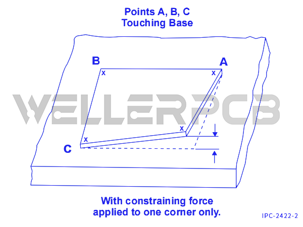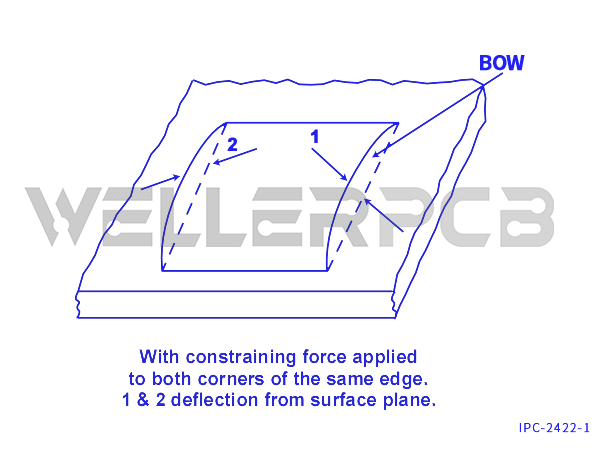
Bow and twist on a bare printed circuit board are two types of deformations that can occur during and after the PCB manufacturing process. It reflects the flatness (or warpage) of a final PCB as defined in the IPC-A-600 standard.
Bow refers to PCB’s deformation with there being a downward or an upward curve in the middle zone of the circuit board. Think of that placing the PCB on a horizontal desktop, there would be a gentle hump or arc in the middle of the circuit board. Twist refers to PCB’s deformation that with in the same plane there being one corner higher or lower height than the other three corners.
The recent increasing development of new components require PCB manufacturing technology to be much more advanced than ever before.
The smaller and fine pitch footprints of SMT (Surface Mount Technology) components drive PCB manufacturers to achieve higher density interconnections, higher pattern accuracy and greater flatness. Even in some complexity electrics deigns, the PCB itself becomes a SMT component that need to be soldered to another circuit board, which requires the PCBs have a rigorous bow and twist performance.
Whether the rigorous flatness requirements from components or that the PCB itself becomes a SMT component, there is a challenge to improve the flatness for both. This challenge has been driving PCB manufacturer and SMT assembly contractor further, and as the sequence that the “bow and twist management” becomes extremely crucial in the manufacturing process.
The poor bow and twist will have negative impacts on the reliability and performance of a final PCBA therefore for some special cases the electronics designer want their PCBs to as perfectly flat as possible.


The smaller and smaller integration of SMT components and the development of high-density interconnections has taken significant challenges of how to control bow and twist in manufacturing PCBs. This article explores the multiple causes of intrinsic and extrinsic bow and twist, outlines various factors leading to these issues, and provides PCB designer and manufacturers insights into strategies for improving PCB flatness and overall performance.

Wht is the Bow and Twist in PCBs
Bow and Twist in PCBs is referring the intrinsic and extrinsic factors that impact the flatness and performance of the circuit board.
The root causes for for bow and twist can be categorized into two groups: intrinsic and extrinsic factors. Intrinsic factors that affects bow and twist is mainly from the PCB manufacturing process that before or during the lamination cure steps, and even there is no permanent corrective action can effect that. Extrinsic factors are mainly from the PCB manufacturing process that after the lamination cure steps, and in most cases the corrective actions can be taken. Some design flaws that affect the bow and twist is also the intrinsic factors, such as unsymmetrical stackup structures, unbalanced copper distribution at the circuit layers, etc.
For the PCB’s extrinsic and intrinsic bow and twist, behind it there are various reasons we should know. Below are some references that how layout and design, production, and external forces and process can directly influence a circuit boards susceptibility to bow and twist:
Production related intrinsic reasons:
Design related intrinsic reasons:
The More You Need To Know
The copper dummy PAD design in the breakaway tab should have the similar copper distribution for each layer. As long as breakaway area is perfectly copper balanced, it will behave differently from the non-perfect PCB, causing potential stress that could lead to a twist in the PCB panel, especially when separating the PCB from the breakaway tabs.
External related extrinsic reasons:
How to test bow and twist, and it’s procedures
The PCB manufacturer should perform necessary tests during the production process to prevent intrinsic bow and twist. When the PCB delivered to the customer’s side with excessive bow and twist, it is important to know whether the root cause is from intrinsic or extrinsic. We recommend the following procedures as a reference:
Bow and twist improvements
When it comes to address bow and twist issues that exceed required tolerances, we must thoroughly investigate the underlying intrinsic causes and fine-tune both design and production aspects that probably impact performance. At first, we must ensure that all relevant production processes are properly under control. And then, we need to review potential improvements and corrections in the manufacturing process that could improve performance beyond standard expectations.
Lamination process
The lamination in PCB manufacturing process is normally tuned to be cost effective and still meet required tolerances. The pressing cycle can be tuned further through extending the cycle times to achieve improved performance.

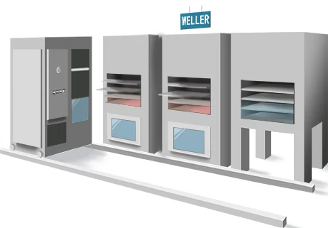
Illustration of a lamination machine. Lamination is the process of permanently bonding together the layers of a multi-layer PCB stack-up under heat, pressure, and specific time.
Prepreg and inner cores
The PCB manufacturer has to find a tradeoff of the use of prepreg between a customer’s specifications and the optimal choice for high performance. To achieve improved stability, the buildup must be 100% symmetric, and the PCB fabrication house need to choose the most robust prepregs and core constructions. The result will more or less affect impedance that needs to be recalculated.
Copper distribution
Copper distribution must be optimized within each circuit layer (power and ground layer) and should be matched within the buildup. The buildup must be symmetric and all pairs of layers on each side of the buildup center should have equal copper weight.
Low-pressure areas
Most designs with a high layer count will have a tendency of low-pressure areas. This could be avoided by adding copper pouring by dummy pads or cross hatched copper.
Split ground planes
Some PCB designs have some layers with so-called split planes that may perform as a bend indicator line, especially if the design have the same pattern in more than one layer through the buildup.
Breakaway areas
The PCB breakaway tab is crucial and the most neglected reason for bow and twist. It is very important for the performance that the coppery on each layer breakaway tab imitate the copper of the PCB itself.
The bow and twist managing for improved PCB performance is a complex work that includes all of above considerations. Monitoring which actions yield the desired effect may need several sample runs. Furthermore, various measures can be performed during the waving soldering and reflow assembly process to improve flatness.
With the support of our experienced technicians and engineers, we possess the expertise and knowledge to support our customers toward achieving superior performance. For assistance with a top bow and twist design, please contact us freely, our experienced engineer will response positively.


