PCB designer often has questions about the difference between IPC class 2 and Class 3. Class 1 exactly exists but it is rarely used. When the boards deliver to our customer manufactured by WELLER, these are always manufactured according to customer required specification, otherwise, the IPC 6012D & IPC-A-600J CLASS 2 applied to all our produced boards.
What is the IPC standard for Printed Circuit Boards?
IPC is an industry standard to reflect the quality level of the print circuit board. There are separately three classes to define the quality of each PCB type of class 1, class 2, class 3. Class 1 is lowest standard and class 3 is highest standard. They are most widely recognized acceptability criteria in electronics industry.
The IPC definition of class 1, class 2, class 3:

Examples of Defect Criteria of Different Classes
The process of PCB manufacturing is extremely complex, involving various factors such as electronics, chemistry, and mechanics. Therefore that is reasonably a number of defects exist in any batch of delivered PCB boards. IPC standards specify which defects are acceptable and which should be rejected. The acceptable defects includes that may impact performance, or these are only in cosmetic issues and will exactly have no impact on performance or reliability.
| Characteristic Inspection | Class 2 | Class 3 | Paragraph in IPC | Weller Capability |
| Etched Annular Ring (External Plated-Through Holes) | Not greater than 90° breakout of hole from land when visually assessed. | The minimum annular ring shall be 50 μm [1.969 μin]. | 3.4.2 and Table 3-5 | Class 2 and 3 |
| Etched Annular Ring (Internal Plated-Through Holes) | Not greater than 90° breakout of hole from land when visually assessed. | The minimum annular ring shall be 25μm [0.984μin]. | 3.4.2 and Table 3-5 | Class 2 and 3 |
| Conductor Spacing | Minimum conductor spacing may be reduced an addi-tional 30% due to conductor edge roughness, spikes, etc., if not specified. | Minimum spacing shall be as specified on the drawing. Minimum conductor spacing may be reduced <20% if not specified. | 3.5.2 | Class 2 and 3 |
| Edge Board Contact, Junction of Gold Plate to Solder Finish (Exposed copper gap) | Copper: 1.25 mm [0.04291 in] | Copper: 0.8 mm [0.031 in] | 3.3.8 | Class 2 and 3 |
| Edge Board Contact, Junction of Gold Plate to Solder Finish (Gold overlap) | Gold: 1.25 mm [0.04291 in] | Gold: 0.8 mm [0.031 in] | 3.3.8 | Class 2 and 3 |
| Final Finish Coverage (Areas not to be Soldered) | Exposed copper on areas not to be soldered is permitted on 5% of the surfaces. Coverage does not apply to vertical conductor edges. | Exposed copper on areas not to be soldered is permitted on 1% of the conductor surfaces. Coverage does not apply to vertical conductor edges. | 3.5.4.7 | Class 2 and 3 |
| Insulation Resistance (As Received) | As received: 500 megohms. | As received: 500 megohms. | 3.10.9 and Table 3-11 | Class 2 and 3 |
| Insulation Resistance (As Received) | After exposure to moisture: 100 megohms. | After exposure to moisture: 500 megohms. | 3.8.4 and Table 3-11 | Class 2 and 3 |
| Minimum Surface Conductor Thickness | Read Minimum Surface Conductor Thickness | 3.6.2.13 | ||
| Negative Etchback | Not to exceed 25 μm [984 μin] if etchback not specified on procurement documentation. | Not to exceed 13 μm [512 μin] if etchback not specified on procurement documentation. | 3.6.2.8 and Figure 3-9 | Class 2 and 3 |
| Plating Thickness, Copper, Blind Vias | Avg. 20 μm [787 μin] Min. 18 μm [709 μin] | Avg. 25 μm [984 μin] Min. 20 μm [787 μin] | 3.6.2.11, Details | Class 2 and 3 |
| Plating Thickness, Copper, Buried Vias >2 Layers | Avg. 20 μm [787 μin] Min. 18 μm [709 μin] | Avg. 25 μm [984 μin] Min. 20 μm [787 μin] | 3.6.2.11, Details | Class 2 and 3 |
| Plating Thickness, Copper, Surfaces and holes | Avg. 20 μm [787 μin] Min. 18 μm [709 μin] | Avg. 25 μm [984 μin] Min. 20 μm [787 μin] | 3.6.2.11, Details | Class 3 |
| Plating, Coating Thickness | Details | 3.6.2.11, | Class 2 and 3 | |
| Plating and Coating Voids in the Hole (Visual) | Copper: one void per hole in < 5% of holes. Finished Coating: three voids per hole in <5% of holes. | Copper: none. Finished Coating: one void per hole in <5% of holes. | 3.3.3 | Class 2 and 3 |
| Solder Resist Cure and Adhesion | Details | 3.7.2 | Class 2 and 3 | |
| Wicking | 100 μm [3,937 μin] maximum | 80 μm [3,150 μin] maximum | 3.6.2.1, | Class 2 and 3 |
| Acceptance Testing and Frequency | Refer to table4-3 | Bare board open and short circuit test |
Most PCB manufacturers here who usually offer attractive prices on their boards apparently looks good quality but propably failure to meet IPC class 2 if withstanding a rigorous quality testing. Therefore you should be very carefully on your decision if your projects applied to dedicated service electronic products. At WELLER we always take IPC class 2 as our bottom quality criteria.
The Design Rules to IPC Class 2 and Class 3
The mechanical design in your printed circuit board will have direct impact on the production yield and the quality of delivered boards.
Below is some typical design guideline reference to PCB layout engineer.
The design rules for annular rings.
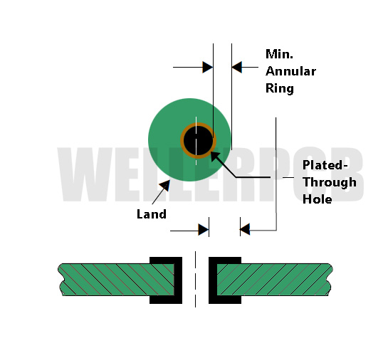
Below table is the annular ring acceptance for IPC class 2 and class 3 from Altium.
IPC Class 2 drill and pad size for 1/2 oz copper
| Drill | Pad | Anti-pad | PCB thickness | Aspect ratio |
| 0.006″ | 0.016″ | 0.026″ | Up to 0.039″ | 6.5:1 |
| 0.08″ | 0.018″ | 0.028″ | Up to 0.062″ | 7.75:1 |
| 0.010″ | 0.020″ | 0.030″ | Up to 0.100″ | 10:1 |
| 0.012″ | 0.022″ | 0.032″ | Up to 0.120″ | 10:1 |
| 0.0135″ | 0.024″ | 0.034″ | Up to 0.135″ | 10:1 |
IPC Class 3 drill and pad size for 1/2 oz copper
| Drill | Pad | Anti-pad | PCB thickness | Aspect ratio |
| 0.008″ | 0.023″ | 0.033″ | Up to 0.062″ | 7.75:1 |
| 0.010″ | 0.025″ | 0.035″ | Up to 0.100″ | 10:1 |
| 0.012″ | 0.027″ | 0.037″ | Up to 0.120″ | 10:1 |
| 0.0135″ | 0.028″ | 0.038″ | Up to 0.135″ | 10:1 |
Drill and pad diameter for various copper thicknesses on IPC Class 2
| Drill and pad diameter | Pad diameter over dril (≤ 8 layers) | Pad diameter over drill (> 8 layers) |
| 1/4 oz copper | 0.010″ | 0.010″ |
| 3/8 oz copper | 0.010″ | 0.010″ |
| 1/2 oz copper | 0.010″ | 0.010″ |
| 1 oz copper | 0.012″ | 0.012″ |
| 2 oz copper | 0.014″ | 0.014″ |
| 3 oz copper | 0.016″ | 0.016″ |
| 4 oz copper | 0.018″ | 0.018″ |
Drill and pad diameter for various copper thicknesses on IPC Class 3
| Copper thickness | Pad diameter over dril (≤ 8 layers) | Pad diameter over drill (> 8 layers) |
| 1/2 oz | 0.013″ | 0.015″ |
| 1 oz | 0.015″ | 0.017″ |
| 2 oz | 0.016″ | 0.018″ |
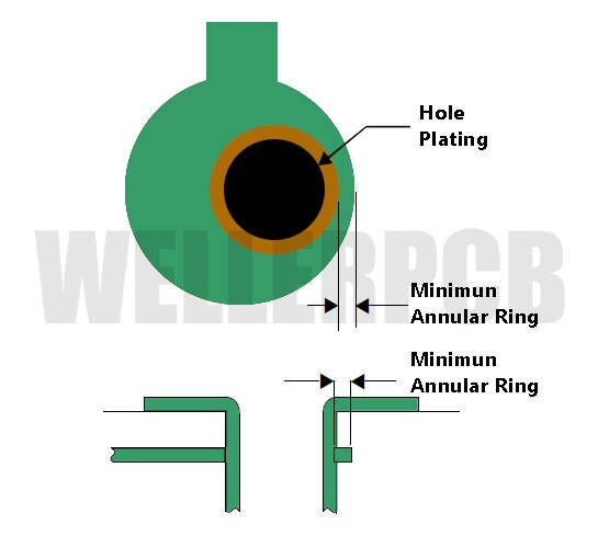
How to calculate the pad size based on the minimum annular ring size
PCB designer need to have a global consideration on some factors including: the via type, PCB layer count, circuit trace width, and manufacturing cost when deciding the via pad size. For example, if you have a large circuit trace width, it is essential to optimize the lager pad size no matter how big is the via size. Another crucial factor is the CNC drill deviation from holes drill process in PCB manufacturing. This occurs when the drill bite misalign with the center of the pad. This takes a result in an insufficient annular ring or causes a ring breakout. Therefore, selecting the right land size is crucial to the final quality of the rings. Below is the formula to calculate the pad size by using IPC-6012 and IPC-2211 standards.

Minimum pad size= a (a=finished hole diameter) + 2b (b=minimum annular ring size) + c (c= fabrication allowance)
Where:
a = Maximum diameter of the finished hole.
b = Minimum annular ring requirements.
c = A standard fabrication allowance.
The fabrication allowance mainly depends on PCB production master tooling and process variations required to fabricate boards. As per IPC-2221, Class C is the highest classification with an allowance limit of 0.2 mm. Additionally, there are different measurement methods for annular ring both in the internal and external layers. The minimum annular ring on external layers is the minimum amount of copper (at the narrowest point) between the edge of the hole and the edge of the land after plating of the finished hole. The minimum annular ring on internal layers is the minimum amount of copper (at the narrowest point) between the edge of the drilled hole and the edge of the land after drilling the hole. Therefore, the annular ring value differ depending on the plating copper thickness.
Minimum Standard Fabrication Allowance for Interconnection Lands:
| Level A: | Level B: | Level C: |
| 0.40 mm | 0.25 mm | 0.20 mm |
The minimum annular ring size required for class 3 boards are as below:
| Minimum annular ring size in inner layers: | Not less than 1.0 mil |
| Minimum annular ring size in external layers | Not less than 2.0 mil |
For example, assuming you have a 10.0 mil diameter via in a class 3 board, the finished hole size will be 8.0mm (2.0 mil plating thickness)
Pad size (external layer)=8+2×2+8=20.0mil
Pad size (internal layer)=10+2×1+8=20.0mil
Likewise, for class 1 and class 2 boards, the minimum annular ring size in the inner layers can be 0 mil. But for external layers, the via plating thickness (1.0 mil) needed to be considered.
To PCB designer, this is one of the safest options of calculating the pad size that meet IPC class specifications. It will ensure your printed circuit boards have less breakout and be more reliable. In IPC class 3, it require the annular ring of PCB board to have the reliable mechanical strength to withstand thermal tension while the circuit board operating in harsh environments. This calculation is only for the minimum annular ring with respect to IPC specifications. But, for the exact design requirement, the PCB designer can increase the annular ring size as much as possible to have a maximum reliability.
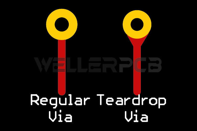
It is necessary to add teardrops at the junction of a pad or via and a circuit trace. The deardrops will let you have thinner circuit traces without reduce the via size. It also can reduce the breakout and improve the manufacturing yield.
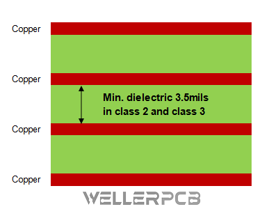
Minimum PCB dielectric thickness requirement
The minimum dielectric thickness between layers is 3.5 mil for both class 2 and class 3. This thickness is to ensure the printed circuit board has enough mechanical strength to withstand the stress without deforming.
Through-hole Plating Requirement
Printed circuit boards specifically required accepted criteria IPC class 3 do not allow any voids in copper plating. A copper void means that some area in the barrel of the hole missing copper plating and exposing the dielectric material of the drilled hole. One void in 5% of the holes allowed in IPC class 2, but no any avoids allowed in IPC class 3. The plating copper thickness for class 2 is 0.8mil (min) and 1.0mil (average), but it is 1.0mil (min) in class 3. WELLER provide the through hole plating of 25um nominal, as standard which equates to IPC class 3. This is 25% more copper plating thickness than that achieved with class 2, and with result in providing greater reliability of the via structure and improved Z-axis expansion performance.
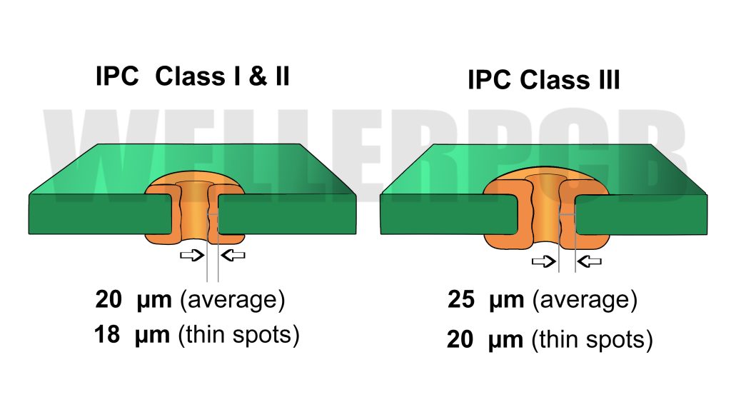
The IPC-6012E specifically defines the following plating minimum requirements for hole and surface and plating (refer to tables T3-4, T3-5, T3-6 below):
| T 3-4: Surface and Hole Copper Plating Minimum Requirements for Buried vias>2 layers, through-Holes, and Blind vias | |||
| Item | Class 1 | Class 2 | Class 3 |
| Copper-average | 20μm [787 µin] | 20μm [787 µin] | 25μm [984µin] |
| Thin Areas | 18μm [709 µin] | 18μm [709 µin] | 20μm [787µin] |
| Warp | AABUS | 5μm [197µin] | 12μm [472µin] |
| Warp | AABUS | 5μm [197µin] | 5μm [197µin] |
| Does not apply to micro-via holes | |||
| T 3-5: Surface and Hole Copper Plating Minimum Requirements for Micro-via holes (Blind and Buried) | |||
| Item | Class 1 | Class 2 | Class 3 |
| Copper-average | 12μm [472 µin] | 12μm [472 µin] | 12μm [472 µin] |
| Thin Areas | 10μm [394 µin] | 10μm [394 µin] | 10μm [394 µin] |
| Warp | AABUS | 5μm [197 µin] | 6μm [236 µin] |
| Warp | AABUS | 5μm [197 µin] | 5μm [197 µin] |
| T 3-6: Surface and Hole Copper Plating Minimum Requirements for Buried Cores (2 layers) | |||
| Item | Class 1 | Class 2 | Class 3 |
| Copper-average | 13μm [512 µin] | 15μm [592 µin] | 15μm [592 µin] |
| Thin Areas | 11μm [433 µin] | 13μm [512 µin] | 13μm [512 µin] |
| Warp | AABUS | 5μm [197 µin] | 7μm [276 µin] |
| Warp | AABUS | 5μm [197 µin] | 5μm [197 µin] |
PCB copper plating thickness is usually measured as an average value from different location of the plated hole. Sometimes the cracks happened once the glass fiber protrusion into the plating of the hole wall. And isolated thick or thin plating is ignored when calculating the average copper plating thickness of the hole.
Voids VS Copper Plating Thickness: IPC Standard
Plating voids usually come out during electrolytic plating stage when the electroless copper plating does not fully cover the internal walls of the though-plated-hole. This is a common phenomenon in the PCB manufacturing process. However, some voids even will take potential risk or affect the final PCBAs reliability. So, IPC-A-600 has specifically presented the accepted criteria of the voids classifications and acceptance criteria.
Target Condition – Class 1,2,3
No voids.
Acceptable – Class 3
No evidence of voids in the hole.
Acceptable – Class 2
No more than one void in any hole.
Not more than 5% of the holes have voids.
Any void is not more than 5% of the hole length.
The void is less than 90°of the circumference.
Acceptable – Class 1
No more than three voids in any hole.
Not more than 10% of the holes have voids.
Any void is not more than 10% of the hole length.
All voids are less than 90°of the circumference.
Nonconforming – Class 1,2,3
Defects either do not meet or exceed above criteria.
Actually, above are just a few different requirements that between IPC Class 2 and Class 3. Usually, we suggest the PCB designer to have a communicate with a professional circuit board fabrication house before starting a new PCB design. Their engineer will provide you necessary guidelines and help you work it right the first time. Once your PCB manufacturing order placed, you should specifically request an inspection report along with a cross-section of your PCB board to make sure that your circuit board manufacturer meet your specifications properly.
The PCB specification requirement verification: Cross-section
Unless you have to select an extremely lost cost PCB fabrication house due to the limited cost budgetary on your project, most printed circuit board manufacturer nowadays perform the basic inspection on PCB manufacturing process, such as AOI, X-ray check and some basic visual inspection. But, these inspections are not always enough to ensure the integrity of a circuit board. To make sure your PCB specification requirements are rigorously met, you must:
Select a professional PCB fabrication house to manufacturer your board:
It is better to have one that qualified by ISO, UL, etc. Generally, these types of manufacturer are professional in engineering and production, and experienced in manufacturing complicated circuit boards (such as HDI, impedance, etc.)
Ask for cross-section analysis and quality inspection report along with the shipment.
To make sure that your PCB manufacturer met your requirements, ask for a cross-section analysis report. A cross-section is the best way to verify the PCB internal structure by destroying a physical circuit board. And then using a microscope to check for various aspects, such as cracks, voids in solder joints, through-hole filling, etc.
General steps for conducting a circuit board cross-sectional analysis:
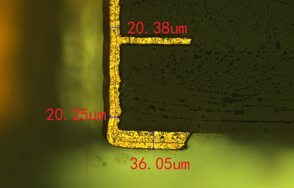
Below is a cross-section of circuit board that required IPC class 2.
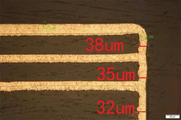
Below is a cross-section of circuit board that required IPC class 3.
At WELLER, we do in-process-quality-check at each step of every batch of PCB manufacturing process. We check for dielectric thickness, plasma etching quality, surface coating finishing thickens, copper thickness, plating thickness, etc. All these done by chemical lab experiment and cross-sections analysis. And if the circuit boards do not meet customer’s specification and requirements, we will reject and scrape it and rebuild another batch. If you need a quality check report, you can ask for a final cross-section along with it. We will send the quality check report with everything we tested and the results in.
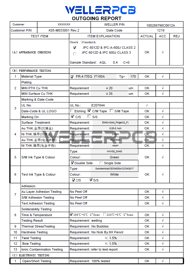
Our outging report looks like as below:
Bare printed circuit board inspection and acceptance criteria
When the PCB comes to the end-use of the product, its inspection criteria is what you should need to take into account when choosing which category your printed circuit board should be classified into. Keep in mind that the higher grade of inspection is one of the factors that raise the final cost when an assembly standard goes up from Class 2 to Class 3.
What is as we see that PCBA is not a simple work. The assembled circuit board needs to properly function once populated with all its active and passive components, electronic materials, and programmed with its proper firmware. Depending on which class your printed circuit board falls into (such as military, industrial, automotive, medical application, etc.), the quality requirements you will have to meet for inspection criteria will differ accordingly. This is why some IPC documents come in to standardize the level of acceptance criteria for each product.
The general inspection methods that PCB fabrication house used for checking circuit board under class 2 or class e including visual inspection, AOI, X-Ray, solder ability test, quadratic element measures, and electrical testing.
However, the quality specs for IPC class 3 printed circuit boards will be much more stringent. Some additional testing such as micro-section analysis specifically required and specific environmental tests like stress, deviation, pressure, vibration, and burn-in tests are also included.
Printed circuit board design and manufacturing standards
Below serial IPC documents set the guidelines and criteria of PCB design and manufacturing:
| IPC series | Standards For |
| IPC 4101 | PCB Laminate selection |
| IPC 2220 | PCB design |
| IPC 6012 | PCB performance and quality |
| IPC-A 600 | PCB inspection |
| IPC-A-610 | PCB acceptability requirements |
| J-STD-001 | Soldering and Process controls |
Typically, there is a misunderstanding that IPC class 3 circuit boards only apply to aerospace field. Usually this is true but these types of circuit boards are not exclusive to aerospace or any other specific industry field. The criteria exactly are based on the specific application of the product. Therefore, Class 3 can also be the criteria for automotive, industrial, military and medical applications.
It is reasonably that a lot of class 3 boards are for aerospace application. The electronic parts operated in space must be highly reliable to avoid any failure that could be very critical. But, for the commercial and consumer market, the tight manufacturing tolerances and stringent inspections would drive up the overall cost of the product, which is just too pricey.
When you ask for manufacturing a class 3 printed circuit board, it means that the PCB has to be produced according to the complete IPC criteria. This implies that the PCB design and printed circuit board manufacturing teams must take account into several factors: like laminate selection, copper plating thickness, surface finishing thickness, annular ring requirements, manufacturing processes, base material qualifications, facilities arrangements, inspection criteria, etc. and set correct design parameters in order to smoothly produce the board that meets all the Class 3 requirements.
As a circuit board designer, it is critical to know the IPC criteria related PCB design and manufacturing that best suit your design. By following the guidelines, you can build a high-quality board while eliminating board complexity and lowering overall costs. Freely contact us if you have any questions related to IPC classes; our PCB design and manufacturing experts will be honor to help you.