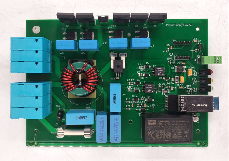
WHat is a Heavy Copper PCB?
A bare printed circuit board can be defined as heavy copper PCB when it’s final finished copper thickness up to more than 2oz (or 70um) in the internal and external layers. So, compared with other normal circuit boards, the heavy copper PCB is made of a thicker layer of the Copper foil sheet.
The Advantages of Heavy Copper PCB
Universal Application of Thick Copper PCB Board
Nowadays, the electronic devices with heavy copper PCB base are widely used for a variety of purposes. For example, in High inductance planar transformers Thermal runaway propagation, high power thermal dispersion, Power control converter system, etc. As well as in PC, automotive, military and mechanical control system, benefitting from the prompt growing of copper-plated sheet. A large number of heavy copper printed circuit boards are also used in:


PCB Designer Must Know About Heavy Copper PCB Manufacturing
PCB designer must know common issues below that often happen in the process of heavy copper PCB manufacturing, which can be eliminated by appropriate work in the PCB layout process.
| Base material: As thick copper PCB is more complex than normal thickness PCB board in it’s manufacturing process (such as in laminate press process, etch process);so the laminate with it’s self-quality is very important to make sure the stable manufacturing flow process. The known brand of good quality laminate base material such as Shengyi, ITEQ(taiwan) is prior to other normal brand material. Some unknown base material will take the cost down, but the potential quality risk hidden in accordingly, such as laminate blister, etc. |
| Specific copper thickness: When you release a heavy copper PCB order to circuit board manufacturer, the specific copper thickness is necessary: such as if 2oz (70uM) specified, the manufacturer maybe use 1oz+extra copper plating so as the finished copper thickness would be 55um (minimum); if 2oz or 70um (min) specified, the manufacture could use base copper 2oz + extra copper plating to start production, so as the finished copper thickness would be 2oz or 70um (minimum). Therefore, specific (nominal or minimum) thickness could be necessary if you want to your PCB to be purposely manufactured. |
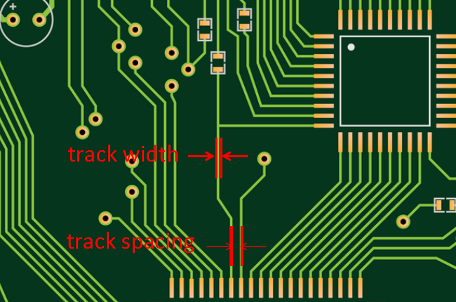
| Appropriate circuit track width/spacing: You must consider your minimum track width/spacing match it’s final copper thickness. Due to etching factors, the minimum track width/spacing differ from it’s final copper thickness: such as 3mil/3mil could be ok for 1oz copper but you could need to release it to 6mil/6mil when the final copper thickness is 2oz. Much more width/gap if the more thick copper thickness needed. You can contact us or your manufacturer for consulting before your work for a heave copper PCB layout. |
| Solder mask color selection: If you have any QFN or QFP component assembled on your heavy copper PCB board, the best option for solder mask color is green instead of any other color such as black, yellow, blue, etc. As green solder mask is more flexible to have enough width of solder mask dam between SMT pads, on the contrary, the other solder mask require more solder mask dam (that means the width of SMT pad sometimes to be limited to narrow width due to expand the solder mask dam spacing between SMT PADs). So, if no special application, please consider green solder mask color as the first option. |
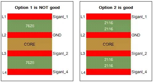
| Stack up design: Heave copper PCB stack up is critical and important for multilayer heavy copper PCB manufacturing. It requires more thick dielectric thickness than that in circuit board with standard copper thickness. Inappropriate dielectric thickness could take preprge starved after laminating process. So as much more resin between copper layers would be very helpful to ensure the high quality of laminate stick. Please refer more Heave copper PCB stack up design study more details. |
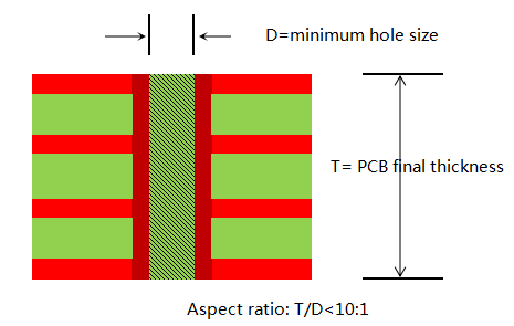
| Minimum hole size: The minimum via hole size must be follow below formulate that: the aspect ratio of PCB thickness/via hole size<10:1; it could take extra risk of circuit open due to that plated copper in the through via hole is insufficient once the aspect ratio >10:1. |
| Heavy Copper PCB Manufacturing Capability | |
| Layer count | 1-60 layers |
| Base material | FR-4 (high Tg, Halogen free),CEM-1,CEM-3, FR-1,FR-2,Aluminum |
| Board thickness | 0.3mm-7mm |
| Max.Finished Board Size | 500mm*500mm |
| Min.Drilled Hole Size | 0.25mm |
| Min.Line Width | 0.10mm(4mil) |
| Min.Line Spacing | 0.10mm(4mil) |
| Surface Finish/Treatment | HALS/HALS lead-free, Chemical tin, Chemical Gold, Immersion gold Immersion |
| Copper Thickness | 2.0-8.0oz |
| Solder Mask Color | Green / Black / White / Red / Blue / Yellow |
| Hole Tolerance | PTH:±0.075, NTPH:±0.05 |
At Weller Technology you can receive an instant quotation for heavy copper PCB manufacturing service for your home or office. So, you don’t have to waste your time looking for the services providers because our experienced technical engineer will send our thorough engineering suggestion along with our quotation sheet.
Weller Technology has specialist people that deliver the best services upon the reasonal prices. What’s more, our team will also provide you with the estimated costs of your project. You can also count on our DFM support service to optimize your design before release it to manufacturing process.