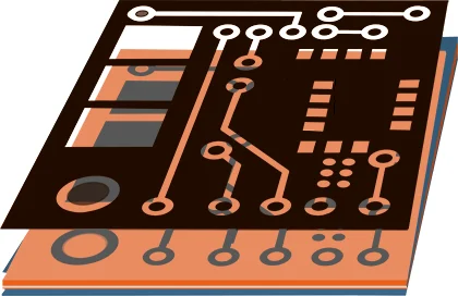
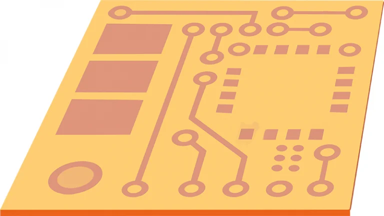
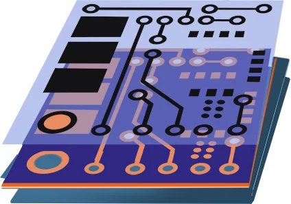
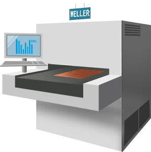
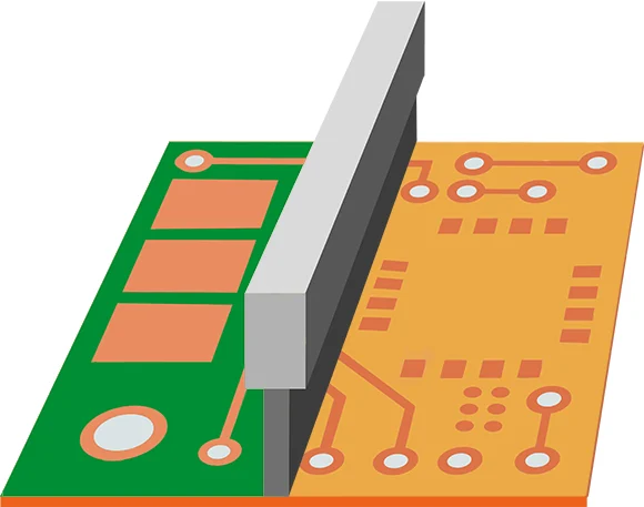
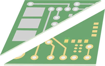
Printed circuit board is the core component to any electronic devices. And, there are many PCB manufacturers in China with offering various of low prices in the market,vary in different quality level accordingly.
But in WELLER, quality and safe production is always the first consideration beginning from prototypes opposite to other suppliers who attract the order by offering lower price via using inferior or unknown low cost materials.
The PCB manufacturing flow chart below presents the ways that how WELLER process is more safe and professional than other suppliers. Such as come core points, DFM review, known brand base material, thick copper thickness in through plated holes, etc.
If you have high complex PCB design and need more details about production process, then please freely contact us and our engineer would be more than happy to present our assist.

Customer provide PCB files ( Gerber file is a best option of document for manufacturer’s CAD or CAM optimizing) along with full PCB specifications such as layer count, base material, copper thickness, surface finishing, solder mask and silkscreen color, impedance or not…. The engineer in the Weller team will perform verify the design and the specification against our manufacturing capabilities. Any change or modification issued in Weller must be officially approved by customer before manufacturing.
Weller’s value: Experienced engineer + the leading PCB pre-production CAM system Genesis 2000 to handle your data to ensure the work in security from the very start of the process. Will not change customer’s design or specification unless get customer’s approval.
Base material is one of the key points that related to final PCB quality especially talking multilayer PCB. The quality of base material is mostly subject to it’s price.
Here are there are many unknown or local brand materials with low prices but unstable quality (multi-problems such as de-lamination defects in multi-layer PCB assembly process and voltage leakage in final functional PCBA operation),some of them even not certificated by UL.
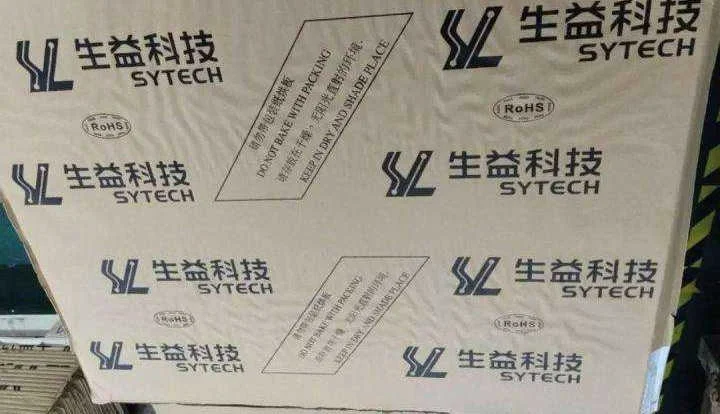
Weller: No matter that it is only some PCS for prototype PCB or big quantities in mass production,unless customer’s prices pressure that have to select poor quality of base materials, or else We only use the base materials public known in industry filed such as Shengyi, ITEQ, Nanya, Kingboard, Rogers, etc. All the base materials used the PCB produced by WELLER must be certificated by UL, rather than the unknown ones, which are out of standard of UL but used by most of other low cost suppliers.
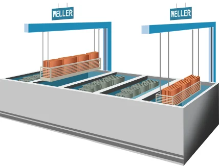
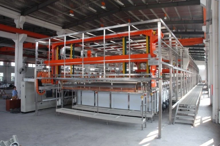
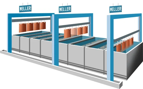
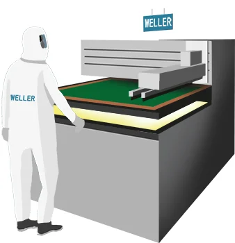
It is also called the inner imagine transferring in a clean room, it is to transfer the PCB circuit image by using an artwork film to the circuit board surface, using photosensitive dry-film and UV light, which will polymerise the dry film exposed by the artwork.
Weller:
The grade of clean room: 100 000;
The high quality of artwork film imported from Japan.
This is to remove the unwanted copper from the working panel by using chemical etching.
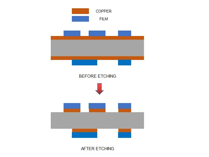
After the unwanted copper has been removed, the remaining dry film is then to be removed off and leaving behind the copper circuitry that matches the circuit design.
WELLER’s Value:
Advanced automatic control etching production line with high deficiency work from start to end without any manual process.
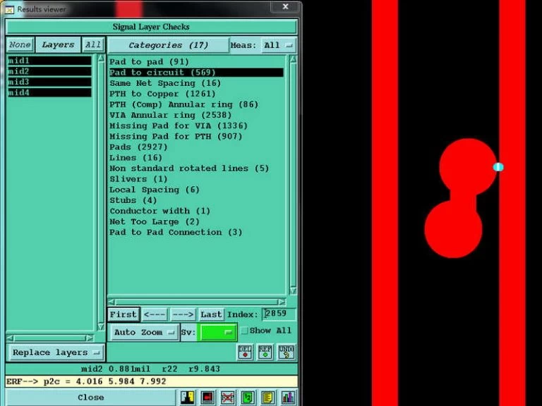
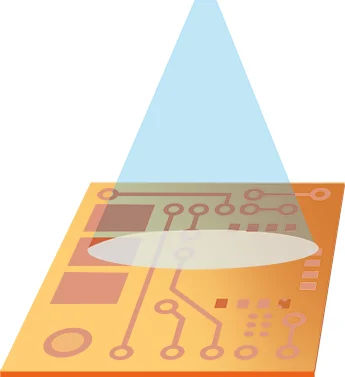
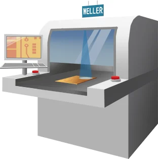
Through scanning of the production circuit board to catch out the defects via comparing the exist circuit against the digital “images” from original design.
The purpose of this stage is to sort out the defects PCB in inner layers production, and do not leave it to next production process.
WELLE’s value:
Latest leading AOI machine+90% automatic running instead of manual scanning work.
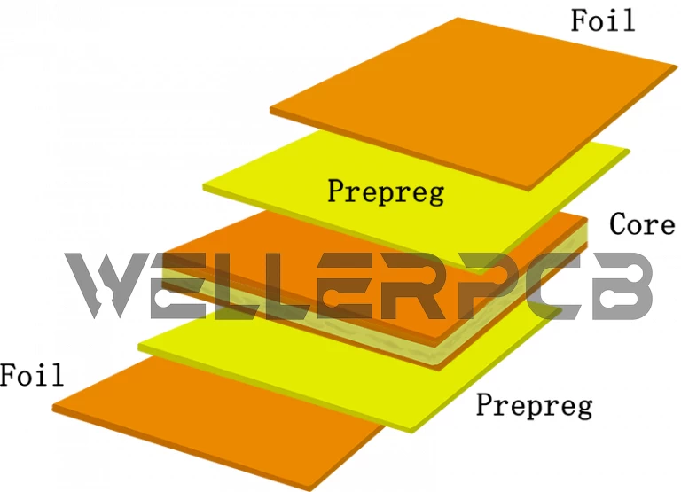
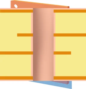
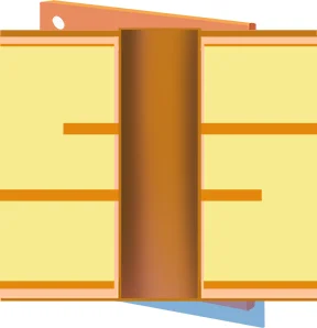
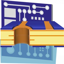
It is to “stack ”inner layers, prepreg (which is for insulation purpose) and copper foil of out layers (top and bottom) together.
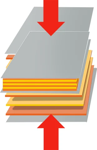
It come out by using a combination of specific temperature (heat and cooling), pressure for a specific time to allow the resin within the pre-preg to flow and bond the layers together to form a solid multilayer panel.
Normally, there are many times of lamination process for some multi-stacked via and blind holes.
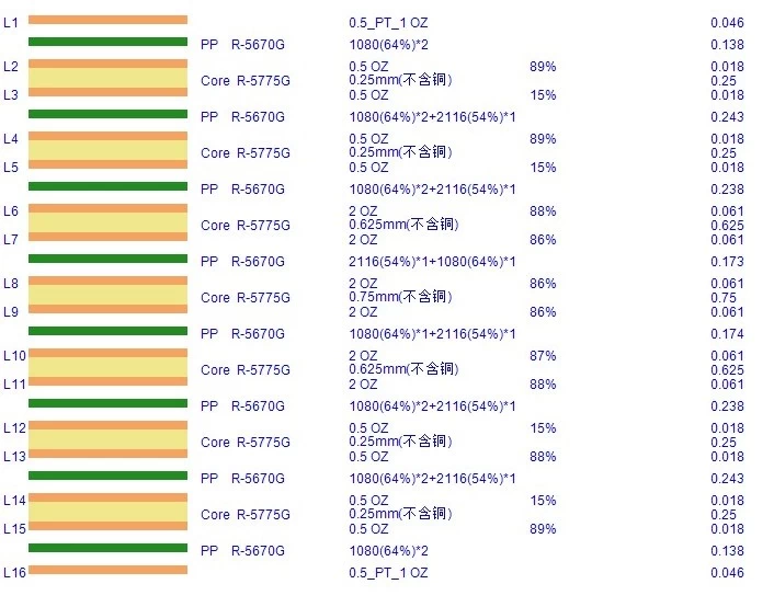
An outstanding PCB stackup design is critical to multi-layer printed circuit board, WELLER will not change customer’s stack up unless get official approval from customer. This action are far more stringent than those of other suppliers. Such as approved stackup design for 16 layers rigid PCB with using Panasonic MEGTRON6 Laminate R-5775.
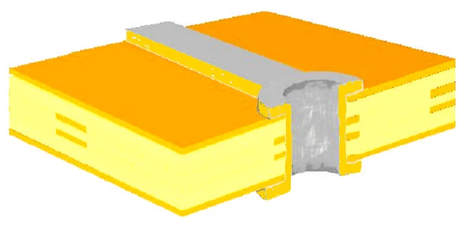
It is to subsequently drill the holes within the multilayer PCB via the drilling machines.
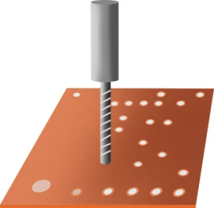
This process must be highly optimised so that it can meet the registration positional accuracy to all of the the inner layer connections.
Eexcept the mechanical drilling process, the drilling can also be done by a laser drill for blind holes (LASER CO²+LASER UV).
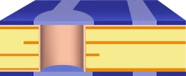
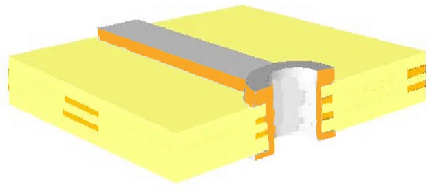
PTH also called Plated Through Hole: the purpose of this process is to plate thin copper (normal thickness is 0.3-0.5um) to the wall of the through holes by a complex chemical process to get the basic electrical connection to the layers.


Panel plating after PTH process is to plate 5-8 um extra copper to the surface of PTH copper. This is to protect PTH copper from damage during the next following up process.
WELLER:
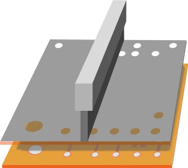
Copper thickness on through plated hole: 25um(min). Which is the same standard of IPC class 3.
Or else, the poor thickness copper on the through plated hole will take risk of open circuit after high temperature of PCB assembly process.
The similar process as the inner layer’s (perform the image transfer by using photosensitive dry film, exposure to UV light and etching). Only with one main difference:the dry film where we want to keep the copper/circuit track will be removed– so as that we can plate additional copper later in the process.
This step of the process is performed in a high grade clean room.
The detail of steps of outlayer imagine process is as below:
Dry-film Resist Coating Outer Layer Panels
The same resist or light sensitive film used on the inner layers is used for the outer layers. The film covers the entire surface including the drilled holes.

Outer Layer Expose & Develop
After dry film lamination the panel is exposed and developed using the same procedure used for the inner layer cores. Clear areas in the film allow light to pass through and harden the resist creating an image of the circuit pattern All of the drilled holes that are exposed will be plated through.
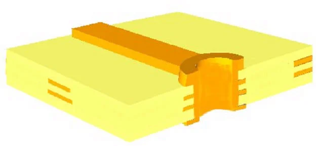
Copper “Pattern” Plate
The electroplating processes that electrically plates copper onto the exposed metal surfaces is next. The copper will be plated up to a thickness of approximately 1 mil (0.001”), depending on the required final finish for the panel.
The copper plating step is followed by plating tin onto all the exposed copper surfaces.

The tin will be used as an etch resist to maintain the copper traces, hole pads and walls during the outer layer etch process.
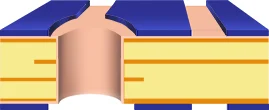
This is second electrolytic plating stage that to electrically plates copper onto the exposed metal surfaces ( in areas without dry film (circuitry)).
By this process,the copper will be plated up to a thickness with and average of 25um / min 20um through the hole. Once the copper has been plated, tin is applied to protect the plated copper(which will be il).
WELLER’s standard copper thickness of through hole is 25um (nominal), which equates to IPC class 3,this thickness can provide much more greater reliability of the via structure and improved z-axis expansion performance.
3 basic steps in pattern plate process:


This is simply a three step process.
The first step is to remove the blue dry film to expose the unwanted copper.
The second step is to etch away the exposed/unwanted copper but now the tin deposit acts an etch resist protecting the wanted copper.
The third and final step is to chemically remove the tin deposit leaving the pads and traces on the panel surface.
Then the tin is chemically removed leaving behind a bare copper and laminate panel. The surface pads, traces and plated through holes are the exposed copper. This is the last step in strip-etch-strip.

Similar with inner layer AOI the imaged and etched panel is scanned and compared to make sure that the circuitry meets design and that it is free from any defects.

WELLER do not allow to repair any welding or open circuit.

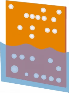
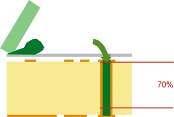
It is to plug the via holes by solder mask or by resin performed in a clean room.(Or fill the via holes with copper,which is another process).
How to do this? By screen printing to push solder mask into holes – a separate operation using an aluminium stencil.
WELLER perform the plugging criteria with 70% filling per hole. This is to eliminate the risk of “broken” circuit path after high temperature in assembly process.
Soldermask ink is coated over the whole PCB surface. By using artworks and UV light we expose certain areas to the UV and those areas not exposed are removed during the chemical development process – typically the areas which are to be used as solderable surfaces. The remaining soldermask is then fully cured making it a resilient finish.
This step of the process is performed in a clean room.
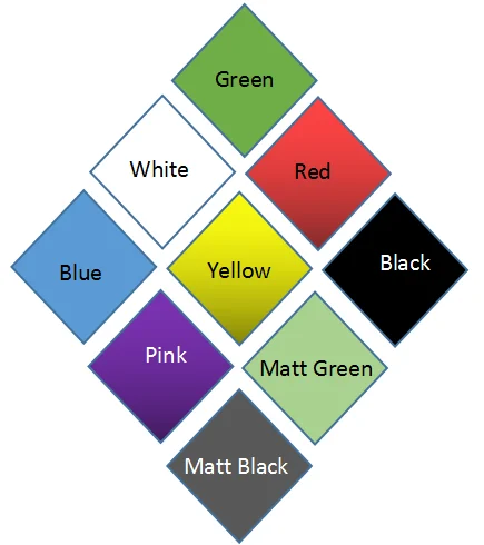
Common PCB silkscreen color: Green, black, white, blue,yellow,pink,red,matte green, matte black.
The primary purpose of the mask is to restrict the areas that will be covered with solder. It also protects panels from contamination, handling damage and possible electrical shorting during assembly and installation.
Importance: With ≥ 5um on the knee of the track and between 10-30um on the surface. The thickness of solder mask is critical to improved electrical insulation and resilience to chemistry or mechanical force that could cause loss of soldermask.
At WELLER,we always keep using high quality of soldermask material such as Taiyo-PSR-4000 to print the PCB board.
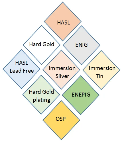
Various of PCB surface finishes are used to coat the exposed copper areas. This is to enable protection of the surface and good soldering-ability.
The various of finishes can include Electroless Nickel Immersion Gold, HASL, Immersion Silver,ENEPIG etc.
Thicknesses and solderability tests are always carried out.
Commonly available PCB surface finishes in Weller (all in house)
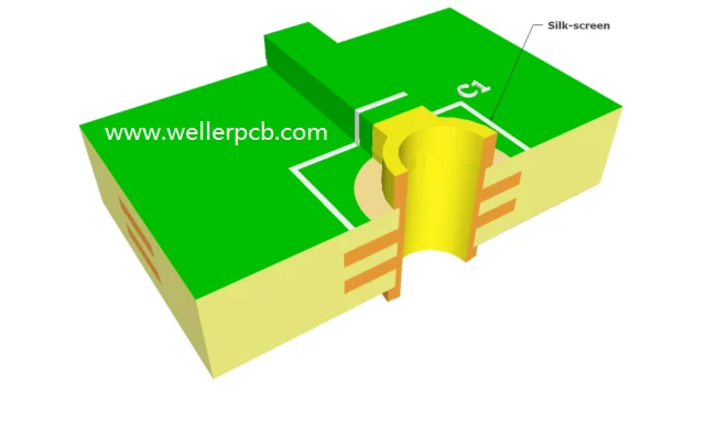
Non-conductive epoxy ink is silkscreened onto one or both sides of the panel depending on the requirements of the customer.Or, it is printed out by laser machine.

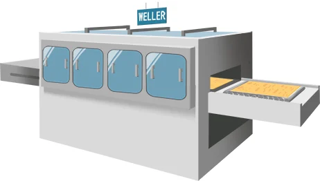
The printing usually dictates the component placement, part number or name, date code, logo or other specified information. PCB Panels are then baked to cure the ink.
Common PCB silkscreen color: White,black,red,yellow.
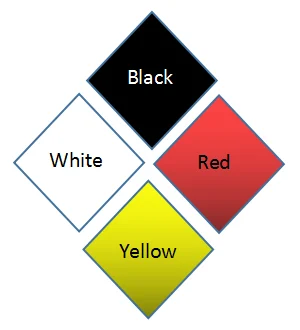
WELLER normally use silkcreen ink Tamura DSR 330 to ensure a high quality of legend printing. And we are upgrade the printing machine to laser printing to get a bettter quality.
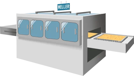
After surface finishing process,then the boards are cut to size on a CNC machine or router.
Most panels have the individual parts routed out into single pieces or arrays of varying sizes. Boards or arrays can also be scored so that they can be easily broken apart after assembly.
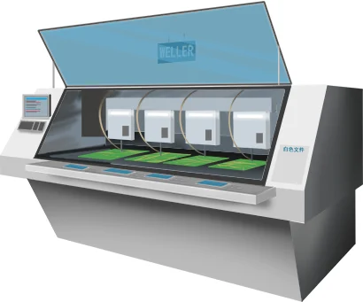
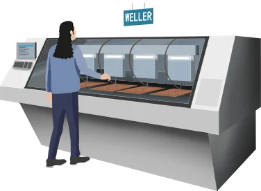
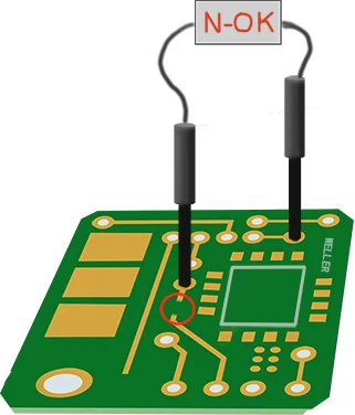
PCB boards are tested for opens and shorts in the circuitry, in one of the last steps of production.
Test programs can be loaded directly onto various types of test machines or used to create specific fixtures and test programs.
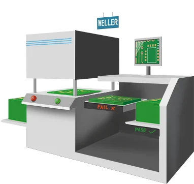
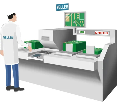
PCB boards are visually inspected to assure they meet our customers’requirements, industry specifications (IPC class 2 or class 3) and WELLER’standards, as well as having the physical dimensions and hole sizes verified with a paper report with shippment to customer.
PCB Boards are vacuum wrapped using specific materials that made from renewable resource materials. To assure the boxes can not be damaged during transport.