What is Hybrid Printed Circuit Boards?
Hybrid PCB is a multi-layer printed circuit board that consisted by two different laminate materials so as to get a best electrical performance and operation reliability where the PCB installed. This is widely used in high-frequency RF applications, such as communications, defense, satellite and aerospace products. The key challenge to PCB fabrication house when manufacturing this type of circuit board is how to well manage the different coefficient of thermal expansion (CTE) properties from different circuit base material in PCB fabrication process.
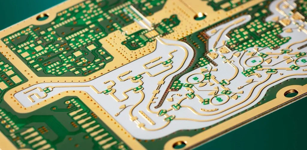
Usually, designing this type of PCB is to combine two different of substrate materials such as FR4, metal core, PTFE or Rogers in one stack up to have all the RF functionality components and non-RF functionality components assembled on the same circuit board which can reduce the PCB size and save the costs.
There are various high frequency materials from some world class laminate material suppliers available for PCB design engineer’s selection, such as Rogers, Arlon, Taconic, Panasonic, and Isola. The materials technical information specifically presented on their laminate datasheet.
Our experience in manufacturing multi-type of hybrid PCBs enable us to have the absolute confidence to provide our customers with most comprehensive supports and services.
Hybrid RF PCBs Laminate Construction Considerations
To produce a printed circuit board stacked with dissimilar laminate material, basically the PCB manufacturer should have the necessary equipment with it’s capability that well accommodate the physical properties of the laminate, and an experienced team that is familiar to some key factors which affect this kind of production. Because of the different CTE value on dissimilar laminate materials (FR4, Rogers, PTFE, Copper core), each material expand/contract at a different rate when it is heated or cooled. This could take significant layer registration issues as one material expands while another material shrinks during elevated thermal exposure (i.e. PCB layers lamination). And it also causes delamination between interfaces of the copper-to-substrate. Therefore, not all materials are suitable to manufacture hybrid PCBs as they are not so friendly to be manufacturable regardless of the excellent performance.
Before starting designing a new hybrid PCB, getting a professional engineering support from your PCB manufacturer will have your design be more convenient to the coming manufacturing process, as the manufacturer are most familiar what material can have best working match. For example, Rogers 4350 serials material are ideal high frequency materials for high frequency applications. But it takes biggest challenge to manufacturing process that it shrinks after the production etch the copper off so the manufacturer need to know how it works in the production process to compensate for this issue.
Typically the hybrid constructions including a loss material like Rogers combined with another core material such as FR4.
Hybrid RF PCBs Stack Up Challenges
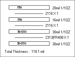
The key application of RF/microwave is it’s excellent ability of staying within the specific tolerances so as that it is easy to achieve the required frequencies. The critical challenge in designing a hybrid PCB stack up is consistently getting an overall PCB thickness requirement between different panels or different PCS in some specific applications. As there is more than one type of material constructed in the stack up, there will be also not only one perpreg used to have the stack up laminated together.
Most of the RF PCB designs have RF signal track layers that have large area without enough remaining copper after etching production process, so as that the manufacturer will use uncommon techniques to assure the enough insulation (prepreg) between the layers and that the final PCB has a consistent overall thickness.
Typically, there are two types of FR-4 prepreg alternatively for rigid printed circuit board stackup, the one is flow and the other is no-flow. The no-flow prepreg is always the best solution to have consistent thickness to the stack up of hybrid PCB but this would add material the overall stack up and potentially change the electrical properties of the entire circuit package. Different PCB manufacturers process work exactly differentially so as that initial involvement is necessary and critical to a one time successful design.

Special Mechanical Features of High Frequency PCBs
There are enough challenges existing in managing the electrical and RF properties of a hybrid printed circuit board, but usually PCB designer desire some special mechanical features to achieve the maximum performance of the entire package, which rise up extra challenges to PCB fabrication process and put difficulties into effective manufacturing cost. A few typical times like:
Odd RF Circuit Board Profile
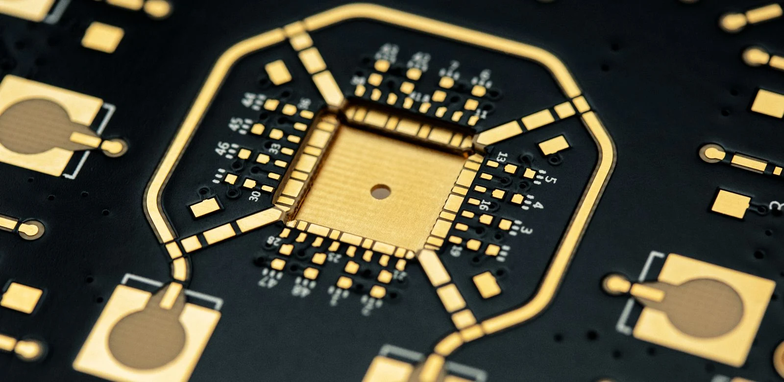
Most RF circuit board embedded into other enclosures or be compatible to other devices which require RF PCB board has many different outlines. That takes extra challenge to PCB manufacturer when routing the outline of the circuit board. As commonly hybrid PCB has it’s special material property opposite to normal rigid FR4 circuit board. Such as the PTFE material is very soft while the Rogers material is very fragile. Therefore, it is quite a sensitive process to PCB manufacturer to deal with a Hybrid design circuit board.
Controlled Depth Routing & Internal Cavity
From below picture illustration we can see what the complex RF Hybrid printed circuit board exactly looks like with internal cut-outs. In order to manufacture out this type of internal cavities, the multiple lamination cycles and controlled depth routing process applied to the Hybrid PCB manufacturing process usually by a router or laser cutter. Specifically both of these processes have direct challenges that can increase the PCB cost and add complexity to the hi-speed PCB design.
The PCB manufacturers use multiple lamination cycles to create these pockets or cavities by routing out the pattern in the PCB production panel and in the prepreg. Once these patterns are completely routing out, then it is very critical to spot on the registration of the patterns, otherwise the bond will failure to pass IPC standards or you will have prepreg leakage where the prepreg comes out from between the layers and could cover a specific RF component or RF track of the circuit board.
For the cavity or cutout that requires a controlled depth process, typically there is very little spacing for any error as the amount of distance between the materials that needs to be removed and the copper feature below it could be as little as 0.0254mm (1 mil).
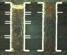
Consistent Plating On Through Plated Hole
The copper plating on PTFE PCB board is not the same as that on traditional FR4 circuit board. The PCB fabricate house must be aware of how these processes impact the hole wall copper plating quality. For PTFE circuit board, typically the plasma etch process is used to “desmear” the holes prior to plating. Absolutely this is an outstanding solution to prepare the hole wall of the PTFE circuit board, but it can also affect more aggressively to FR4 PCB and create an uneven surface which will then turn into uneven plating copper in the hole wall which can cause plating voids or potential electrical failure.
Another common future in high frequency printed circuit board manufacturing process is plugging vias, to plug both internal and external with conductive material to dissipate heat. In order to keep the properties with it’s tolerance and have a consistent amount of material in each plated hole it is very critical to ensure that the holes are properly drilled, thoroughly cleaned, and plated greatly prior to filling.
As all of the materials have different characteristics and various density features, nothing is better than experience in manufacturing Hybird PCBs.