We are a trusted partner with proven professionalism and experience to provide high-quality, reliable, fast-turn services and solutions to our global customers.

10+ Experienced Engineers Team
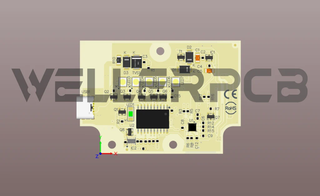
With not big but powerful engineering team plus using leading PCB design software Allegro Cadence and Altium Designer to help PCB designers develop and manufacture electronics products faster and more efficiently.
1 of team leader has 10+ years experience in design high speed PCB , 3 of them has 5+ years related experience in design communication PCB, 5 of them has 1+ years experience.
10+ Years Technology Accumulation
5000+ part numbers PCB design/layout per year
100+ technology training courses per year
Multi-customer’s reputation rewarded
Revolves around focus on Cadence PCB layout
Professionalism in SI, PI, EMC, PCB, DFM.
Revolves Around Focus On Quality
All our PCB design and layout follow rigorous quality system upon check list including layout, wiring, high-speed, impedance calculation, thermal design, structure and self-audit policy, as well as comprehensively checking the schematic of design, DFM, DFT, EMC, thermal design, etc.
Quick Turnaround PCB Layout Service
Our professional and experienced team can provide 7X24 hours services and help to complete your projects or satisfy orders quicker than usual from design to physical prototypes, and without compromising quality.
WELLER have experienced engineers who specialize both in Cadence and Altium software can support you to simply complex designs from concept to manufacturing.

At Weller, we always assign high skilled electronic engineers to support our customer with electronic product design and development meeting the standard IPC 7351. We keep doing right things with correct understanding the customer’s requirement, technical component verification to proceed with impedance matching for signal and thermal LOSSES and BER (Bit Error Rate), timing and frequency analysis. All our PCB layout designs are following as specific guidelines per IPC222X. We also involvingt in Benchmarking and reverse engineering process to track the right path of its procedure and standard.