0.4mm Fine Pitch BGA PCB Design Guidelines
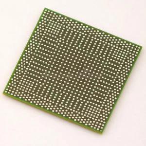
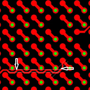
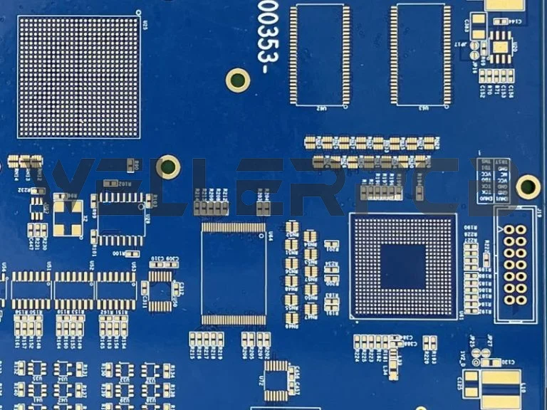
Nowadays, more and more precise electronic components are widely used in some advanced electronics devices, such as fine pitch FPGA component from Xilinx. But accordingly this take extra challenges to PCB designer and PCB manufacturing’s capability when the design has many limits in spacing of tracks, plated holes, electronics performance, etc.
Now, we simply discuss the PCB design guideline for a 0.4mm fine pith BGA component to facilitate in PCB manufacturing process.
Standard Guideline Points:
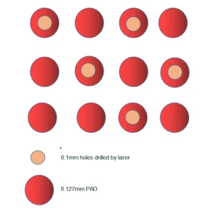

Technology Map for 0.4mm Pitch BGA PCB Design
Advanced Technology Limitation for 0.4mm BGA PCB Design
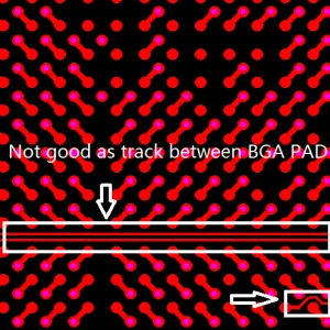
| Item | Inner layer design without tracks between holes | Inner layer design with some tracks between holes | Outlayer design without tracks between holes | Out-layer design with some tracks between holes |
| Drill hole size (mil) | 6.0 | 4.0 | 6.0 | Design deed to be exactly evaluated case by case |
| Track width (mil) | 2.00 | 2.00 | / | |
| Spacing between hole and the track (mil) | 3.87 | 4.87 | / | |
| Annular ring size per side (mil) | / | 2.50 | 3.00 | |
| Other notes: | PCB thickness<=1.20mm; base copper in inner layers: <=0.5oz | PCB thickness<=0.80mm; base copper in inner layers: <=0.5oz | PCB thickness<=1.20mm; base copper in out layers: <=0.5oz | |
| 1. Can only make prototypes 2. Must be symmetrical stack-up design 3. Layout count <= 6L | ||||
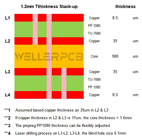
1.2 mm Stack-up Guideline (only for 4L):
1.20 mm Stack-up Guideline (only for 4L HDI)
| 1.2mm thickness stack-up design reference | Thickness | |||||||||
| L1 | Copper | 8.5 | um | |||||||
| PP 1080 | ||||||||||
| TU-7689 | ||||||||||
| L2 | Copper | 35 | um | |||||||
| Core | 900 | um | ||||||||
| L3 | Copper | 35 | um | |||||||
| TU-7689 | ||||||||||
| PP 1080 | ||||||||||
| L4 | Copper | 8.5 | um | |||||||
| **1 | Assumed based copper thickness as 35um in L2 & L3 | |||||||||
| **2 | If copper thickness in L2 & L3 is 17um, the core thickness = 1.0mm | |||||||||
| **3 | The prepreg PP1080 thickness can be flexibly adjusted | |||||||||
| **4 | Laser drilling process on L1-L2, L3-L4; the blind hole size 0.1mm | |||||||||
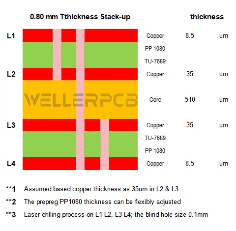
0.8 mm Stack-up Guideline (only for 4L):
0.80 mm Stack-up Guideline (only for 4L HDI)
| 0.80mm thickness stack-up design reference | Thickness | |||||||||
| L1 | Copper | 8.5 | um | |||||||
| PP 1080 | ||||||||||
| TU-7689 | ||||||||||
| L2 | Copper | 35 | um | |||||||
| Core | 510 | um | ||||||||
| L3 | Copper | 35 | um | |||||||
| TU-7689 | ||||||||||
| PP 1080 | ||||||||||
| L4 | Copper | 8.5 | um | |||||||
| **1 | Assumed based copper thickness as 35um in L2 & L3 | |||||||||
| **2 | The prepreg PP1080 thickness can be flexibly adjusted | |||||||||
| **3 | Laser drilling process on L1-L2, L3-L4; the blind hole size 0.1mm | |||||||||
Important Notes to Surface Treatment
Important notes to circuit board surface treatment for 0.4mm fine pitch PCB:
PCB Surface Treatment Design for 0.4mm Fine Pitch Components
| Surface finishing | Options | Rmark |
| HAL(hot air solder leveling) | No-X(the surface is not so smooth so it will take trouble in soldering) | × |
| HAL Lead free | No-X(the surface is not so smooth so it will take trouble in soldering) | × |
| Immersion gold | Good-√ | √ |
Important notes to PCB solder mask for 0.4mm fine pitch BGA components:
If you need a customized stack-up for 6L (or above) PCB board and have more questions to us, please contact us by service@wellerpcb.com.