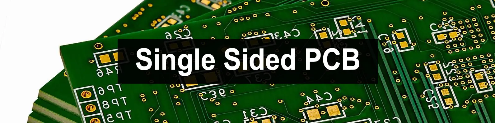
What are Single Sided PCBs?
Single sided PCB, as known as one layer circuit board, which is a printed circuit board with only one copper layer of conductive material above the substrate. And also the electronic components mounted on one side of the board and the conductive track connected on the other side. So, it is called the one layer printed circuit board, too.
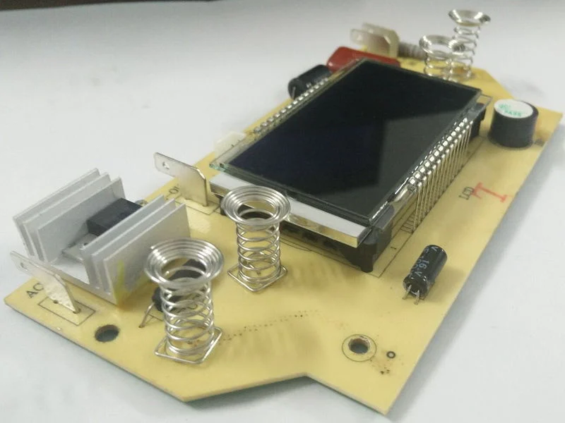
Due to that there is only one copper conductive layer, which is much easier in PCB manufacturing process and with lower cost than that in double sided PCB boards or multi-layer circuit boards. Therefore, these types of circuit boards are commonly used in a wide variety of consumer electronic devices with variety of applications, including: camera systems, printers, radio equipment, calculators, and much more.
Track back it’s initial story, the first single printed circuit board was made in the USA In the 1950s.
Know about Single Sided PCB Stack Up
A single sided PCB design composed by conductive and insulating layers.
In a one layer copper PCB stack up, a single copper conductive layer of copper tracks next to a substrate.
When using such a printed circuit board, an electric component connects to one side of the board. On the other hand, the other side of the circuit board shows the entire etched circuit tracks.
The stack-up design in a single copper layer PCB helps you to construct a stronger electric circuit through layers of PCB board.
Another thing is that it helps the electronic designer to minimize the circuit’s radiations.
What is the Single Side PCB Layer
Commonly, the single sided PCB manufacturing process is very simple to only use the layers of conductive and non-conductive materials.

Substrate material:
Substrate material:
Similar as multi-layer PCB board, different boards of single sided PCB also can have different copper thicknesses. Such as 1oz, 2oz, 3oz, etc.
The Reason to Choose Single Sided PCB Boards
Some crucial advantages determine that most electronic designer love to use them as a PCB design:
The Universal Applications
Single layer PCB has universal applications. Mostly, you can use them in simple or even in complex devices such as:
Design Suggestion that Affect the Cost
The physical design and manufacturing process of a single layered PCB determine its cost mostly. Usually, the single sided PCB cost depends on the following factors:
Why Choose Weller Technology for Your PCB Project
Reasonably that Weller Technology should be your trusted, ideal single sided PCB manufacturer upon our 20+ years manufacturing achievement and experienced team and skilled workers.
Some basic reasons below that could be our crucial advantages that others do not have: