Smooth PCB assembly process is based on the production data of initial PCB design and specification of PCB fabrication. An excellent PCB design work will facilitate subsequent circuit board assembly processing (improving production efficiency, reducing the defect ratio, etc), while incomplete design will affect the processing process and even affect the quality of the final complete assembly product. So what critical factors on PCB design will affect latter circuit board assembly processing? Here is some common issues that circuit board designer need to have an attention on.

2024/08/Smooth-PCB-fabrication-and-assembly-process.webp

There should be no silk screen overlapped on the soldering position.

The silkscreen on the SMT PAD will affect the assembly quality (preventing the solder ability).

2024/04/PCB-Impedance-coupons-design-guidelines.webp

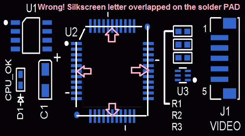
Not good design that silkscreen placed on SMT PAD

However, sometimes the silkscreen mark for some critical ICs is necessary due to that it can be used to identify the deviation of solder quality (especially for some high precious QFN components soldering). In this situation the IC’s edge mark can be put the corner of the SMT zone to avoid any overlapping issues to soldering PAD.

2024/04/PCB-Impedance-coupons-design-guidelines.webp

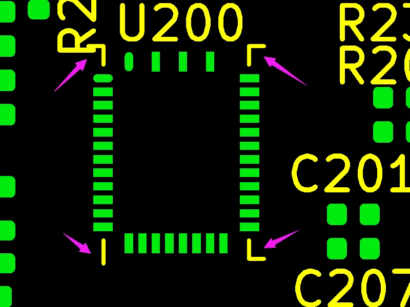
Adjust the IC edge mark to avoid silkscreen on SMT PAD

The minimum spacing between copper foil and board edge is 0.5mm, the minimum distance between component and board edge is 5.0mm and the minimum distance between pad and board edge is 4.0mm.

Necessary of Fiducial mark and Tooling holes:

Fiducial mark (highlighted by red arrow in below picture) is necessary to be placed in single PCB (for single unit PCB) or on the tabs of a panel (PCB produced in a panel). It is used on assembly machines as the reference position for a paste printing machine or a pick-and-place machine to ensure a precise electronic components soldering operation in the PCB assembly process. Normally the minimum diameter of a circular fiducial mark is 1.5 mm with 3.0mm solder mask opening area locates on a 10mm width break-away tab (or on the some places in a single PCB).

2024/04/PCB-Impedance-coupons-design-guidelines.webp

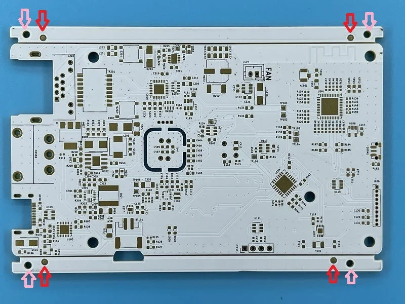
PCB fiducial mark and tooling holes

Tooling holes (highlighted by pin arrow in above picture), normally which is a non-plated hole with a typical size 3.0mm under quantity of 3 pcs at least to be placed on the single circuit board or on the tab of a PCB panel. This is use to fix the printed circuit board not to freely move during some specific PCB manufacturing process such as electronic test process and outline profile process. This is necessary holes for convenience to PCB fabrication and manufacturing process.

When designing the double-sided circuit board, pay attention to the components of the metal shell. When the shell is in contact with the printed board when DIP, the solder pad on the top layer cannot be opened, and it must be covered with solder mask ink or silk screen ink.

Do not place the jumper track under the IC, motors, potentiometer, or other components with large metal shells.

Electrolytic capacitors can not touch heat-generating components, such as high-power resistors, therm resistors, transformers, radiators. The minimum spacing between electrolytic capacitors and radiators is 10 mm, and the interval between other components and radiators is 2.0 mm.

Large components (such as transformers, electrolytic capacitors with a diameter of more than 15mm, sockets with large currents) should increase the pad.

The ideal minimum track width/spacing: 0.1mm/0.1mm; or else it will take extra challenge to PCB fabrication capability and it’s manufacturing cost will raise up accordingly while the track width/spacing is less than 0.1/0.1mm. Of course, if your final electronic product is for a high integrated circuit design and has the limited physical size to PCB circuit board, you have to consider less track width/spacing and the manufacturing cost is at a reasonable range.

PI stiffeners

Track Spacing

FR4 stiffeners

Track width

There should be no copper plane (except grounding required) and components (or as required by the structural drawing) within 5mm of the screw hole radius.

The pad size (diameter) of the general through-hole for mounting component is twice of the hole diameter. The minimum size of the double-sided board is 1.5mm and the single-sided board is at least 2.0mm. If round pads are not available, waist pads can be used.

If the center distance of the pad is less than 2.5mm, the surrounding pad should be wrapped with silk screen ink, and the width of the silk screen ink is 0.2mm.

For components that need to be soldered through the tin furnace, the pad should be opened away from the tin position. The direction of the pad is opposite to that of the tin, which is 0.5mm to 1.0mm. This is mainly used for the back-welded pad in one side to avoid blocking when passing the furnace.

In the large size PCB design (more than about 500 square cm or more), in order to prevent the PCB board from bending when passing through the tin furnace, a 5mm to 10mm gap should be left in the middle of the PCB board without components (can be routed) to be used to add bending bars to prevent bending when passing through the tin furnace.

In order to reduce the risk of short circuit of solder joints, all double-sided vias do not open solder mask windows.

Keep enough physical spacing between SMD components or through hole soldering components, so as  to avoid any potential edge-overlapped issues, or else which will take extra trouble to SMD assembly process(the deviation soldering issues). Deviation soldering ofthen come out due to narrow spacing between SMD components

PI stiffeners

Too close

FR4 stiffeners

Narrow spacing

PI stiffeners

Narrow spacing

The above items is common PCB design factors that directly affect PCB assembly processing, which the PCB layout designer need to know. If you have any other engineering questions please feel free to send your concerns to our email: service@wellerpcb.com, we will response within 24 hours.