
Single Sided Printed Circuit Boards: A Simple, Cost-Effective Solution
In the complex world of electronics, where multi-layer PCBs with dozens of layers power advanced devices, the humble single sided printed circuit board remains a fundamental and incredibly important component. It’s the simplest type of PCB, serving as the foundation for countless electronic devices we use every day.
For engineers, hobbyists, and product developers working on less complex projects, understanding the design, benefits, and ideal use cases for single-sided PCBs is crucial for making informed, cost-effective decisions.
What is a Single Sided PCB?
A single layer PCB, as the name implies, has conductive copper traces on only one side of the substrate (base material, often FR-4). The other side is typically used for housing the electronic components. The copper layer is etched to form the desired circuit pattern, and a protective solder mask and silkscreen layer are applied on top for insulation and labeling.
This simple structure makes them the most straightforward PCB type to design, manufacture, and troubleshoot.

Track back it’s initial story, the first single printed circuit board was made in the USA In the 1950s.
What is a Single Sided PCB?
Why would you choose a single-sided design over a more complex multi-layer alternative? The advantages are significant for the right projects:
Low Cost:
This is the most compelling benefit. With only one layer of copper and a simple PCB manufacturing process, single sided PCBs are the most affordable option by far, especially for large production runs.
Simple Design and Manufacturing:
The design process is less error-prone, and the etching and drilling processes are straightforward. This leads to faster production times and higher first-pass success rates.
Ease of Assembly and Repair:
With components on one side and traces on the other, it's incredibly easy for automated machines or hobbyists to assemble these boards. Debugging and repairing circuits are also simpler due to the lack of overlapping traces.
Reliability for Simple Circuits:
With fewer potential points of failure like vias (holes that connect layers), well-manufactured single-sided boards are highly reliable for their intended applications.
Common Applications and Uses
You might be surprised by where you can find single-sided PCBs. They are the workhorses of simple, low-cost electronics:
- Consumer electronics: Calculators, remote controls, radio receivers, and LED lighting.
- Power supplies: Relays and solid-state power converters.
- Industrial sensors and controls.
- Automotive applications: Dashboard switches and simple sensors.
- Educational kits and hobbyist projects (e.g., Arduino shields for beginners).
- Vending machines and household appliances.
Single Sided vs. Double Sided PCB: What's the Difference?
The core difference is in the name. A single sided PCB has conductive copper on one side, while a double sided PCB has copper traces on both sides of the substrate. These two layers are connected by small holes called “vias.”
This allows double-sided boards to host more components and much more complex circuitry in a smaller space. While they are more versatile, they are also more expensive to design and manufacture. For many applications, the added complexity and cost of a double-sided board are unnecessary.
Design and Manufacturing Considerations
Designing a single sided PCB requires careful planning because the traces cannot cross over each other without a short circuit. This often requires a creative use of jumper wires to “hop” over another trace—a feature that is inherently built into double-sided boards with vias.
When working with a single sided pcb manufacturer, it’s essential to provide clean Gerber files with clear specifications for the solder mask and silkscreen. Despite their simplicity, design for manufacturability (DFM) rules still apply to ensure a smooth and cost-effective PCB production process.
01 Know about Single Sided PCB Stack Up
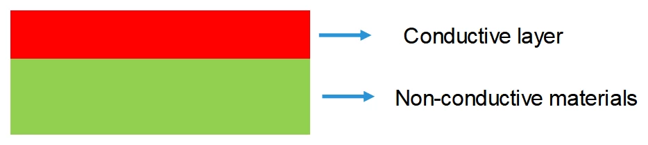
A single-sided PCB (Single-Sided Printed Circuit Board) is a fundamental and cost-effective circuit board design consisting of one conductive copper layer laminated onto an insulating substrate. This simple stack-up features all electronic components mounted on one side of the board, while the opposite side reveals the etched copper circuit traces.
Due to its straightforward structure, single-layer PCBs are highly efficient for simple circuits, reducing manufacturing complexity and minimizing electromagnetic radiation. This makes them an ideal choice for basic electronic applications where reliability and affordability are key.
02 What is the Single Side PCB Layers
The single-sided PCB manufacturing process is notably straightforward, utilizing just one conductive copper layer laminated to an insulating substrate, which streamlines production and reduces costs for simple electronic applications.
03 Substrate material
The foundation of any single-sided PCB is its substrate, a rigid base material typically crafted from fiberglass. This insulating core provides the circuit board with essential structural integrity, rigidity, and a compact form factor.
Crucially, the specific properties of the chosen substrate material—such as FR-4, CEM-1, or aluminum—directly determine the performance, application, and classification of the final single-sided printed circuit board.
04 Copper Layer
A thin layer of conductive copper is laminated onto the substrate, forming the essential circuitry of the single-sided PCB. This copper layer is precisely etched to create custom circuit traces, providing the electrical pathways for current to flow between electronic components soldered to the board.
Similar to multilayer PCBs, single-sided PCB boards are also available in various copper weights, including standard thicknesses such as 1oz, 2oz, and 3oz, to meet different electrical and thermal requirements.
Conclusion: The Right Tool for the Job
While they may not have the glamour of high-density interconnect (HDI) PCBs, single sided printed circuit boards are a vital and irreplaceable part of the electronics industry. Their unbeatable cost-effectiveness, simplicity, and reliability make them the perfect choice for a massive range of low-density electronic applications.
When starting your next project, consider the circuit’s complexity. If your design can be efficiently routed on one layer, opting for a single-sided PCB can dramatically reduce your costs and lead times without sacrificing performance.
Looking for a reliable single sided PCB manufacturer for your project?
Contact Us Today for a quick quote and experience fast, affordable, and high-quality prototype PCB manufacturing.


 Equipment for PCB Assembly Quality Inspection")

