
Introduction
While general discussions on multi-layer PCB lamination exist, mastering the 4-layer PCB stack-up is key to solving real-world design challenges. We move beyond basic theory to explore common stack-ups like the standard “Sig/Pwr/Gnd/Sig” model, providing actionable insights to enhance your next design’s signal quality and reduce electromagnetic interference.
Master the pros and cons of the common 4-layer PCB stack-up to make informed design decisions. This article provides a detailed analysis of its key advantages and inherent limitations. We will answer two critical questions for every PCB designer: how to choose the optimal stack-up for signal integrity, and how to avoid common EMI pitfalls.

Key words:
Stack-up (laminate structure):
It means for layer sequence of copper layer and insulation dielectric sequence,correspondingly including it’s thickness such as:dielectric thickness,copper thickness.
Core(copper clad laminate):
The skeleton of a printed circuit board,one double-sided copper clad PCB board, Usually it refers the double-sided panels that can be used as producing the PCB inner layers.
The Essential 4-Layer PCB Stack-up: Power, Ground, and Signal Layers
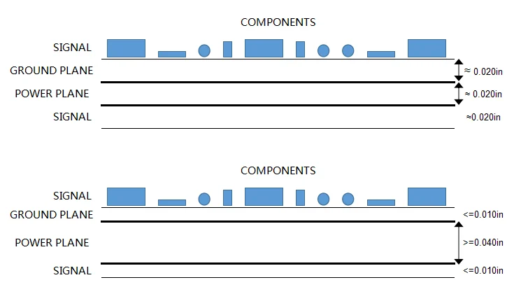
As illustrated above, this standard stack-up features signal layers on the top and bottom, with dedicated internal power and ground planes. This structure provides an immediate, low-impedance return path for currents directly adjacent to each signal trace.
The primary benefit is a dramatic reduction in current loop area and path inductance. This translates directly into superior performance: significantly lower noise interference and minimized signal radiation (both common-mode and differential-mode). In fact, a four-layer board typically achieves a 20 dB reduction in radiation compared to a two-layer board of similar functionality.
The key to this performance is proximity. Keeping the signal layer close to its reference plane (power or ground) is critical. For optimal Electromagnetic Compatibility (EMC) and reduced EMI, the dielectric thickness between a signal layer and its reference should be minimized. While the stack-up in Fig. 1 is electrically functional, the configuration in Fig. 2 offers enhanced performance due to its thinner dielectric, creating a tighter coupling between signal and reference layers. Both configurations can meet basic EMC requirements and achieve the same final board thickness (e.g., 1.6mm).
Limitations of the Traditional 4-Layer PCB Stack-up
The standard 4-layer stack-up (with Top/GND/PWR/Bottom layers) excels in many scenarios but has a critical limitation: it struggles with layer changes for high-speed signals( once the signal track changed to layer4 from layer 1,refer below fig-3).

The red line traces the path of the signal current, and the blue dashed line shows the return current path. When the signal frequency is high enough and the dielectric between layers is thin enough, the return current can use the interplane capacitance to navigate from the power to the ground layer. Because no direct connection exists between these two planes, this creates a break in the path—an point of impedance—as depicted in Fig. 4.

Insufficient interplane capacitance presents a significant problem: it results in high impedance between the power and ground planes. When this occurs, the return current is forced to find a longer, alternative low-impedance path, which dramatically increases the loop area. This large loop acts as an antenna, leading to electromagnetic interference (EMI) that can disrupt nearby signals.
This issue is particularly prevalent in standard 1.6mm (0.062 inch) thick stack-ups, as shown in Fig. 1 and 2, which typically exhibit poor intrinsic capacitance. While signal integrity may not be severely impacted, EMI is a near-certainty. Consequently, avoiding layer changes for high-speed signals—especially clocks—in such stack-ups is critical.
When a layer change is unavoidable, a decoupling capacitor must be placed near the via to bridge the power and ground planes, providing a low-impedance return path. However, this solution is frequency-dependent. As signal frequencies exceed 200-300 MHz, the capacitor’s parasitic inductance causes it to resonate, rendering it ineffective.
Therefore, while decoupling capacitors are a valid fix for signals below 200-300 MHz, addressing the root cause by increasing the interplane capacitance is essential for managing higher-frequency signals.

Even without layer changes, insufficient interplane capacitance poses a significant risk to power integrity. Modern ICs demand substantial transient current during fast switching events. As signal rise times fall below 500ps, the power supply’s effective frequency increases, pushing beyond the useful range of standard decoupling capacitors. When this happens, parasitic inductance dominates, causing capacitors to resonate and fail as effective charge reservoirs.
This is where interplane capacitance becomes critical. Acting as a inherent, high-frequency distributed network, it provides a low-impedance charge source where discrete capacitors are ineffective. For high-speed designs, this intrinsic capacitance is not just a complement but a necessity for stable power delivery. It is important to note, however, that achieving this by specifying a thinner dielectric can increase fabrication costs.

Comparative Analysis of Improved 4-Layer Stack-ups
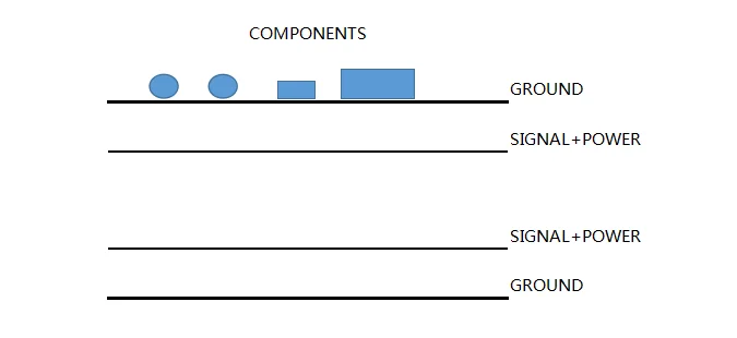
The conventional stack-ups in Figures 1 and 2 mandate an adjacent reference plane for each signal layer to minimize the return path. From this perspective, the stack-up in Figure 6 is suboptimal for the top layer, as component placements can disrupt the ground plane’s integrity. However, its third layer serves as an excellent routing channel, backed by a solid ground reference.
Both improved stack-ups (Fig. 6 & 7) utilize dual ground planes, establishing a low-impedance reference that suppresses common-mode radiation. Figure 6 offers a distinct advantage: its ground planes envelop the inner signal layer, forming a shielded structure that effectively contains high-frequency noise. Stitching these planes with vias can create a Faraday cage, further enhancing EMI suppression—a feature absent in Figure 7.
A key trade-off is the absence of a dedicated power plane. Power must be routed using copper pours, demanding careful network optimization. If components and signals can be predominantly confined to the top layer, Figure 7 is highly recommended due to its pristine ground plane. For more complex layouts, Figure 6 provides a viable alternative.
The distributed copper on the power layer, positioned close to a ground plane, generates significant interplane capacitance. Some designers argue that the decoupling achieved in these configurations surpasses that of the traditional power-ground plane pair. When combined with standard decoupling capacitors, this results in superior high-frequency power performance.
Finally, a major benefit of these stack-ups is the facilitation of seamless high-speed layer changes. With a consistent ground reference on both sides of the signal and well-connected vias, the return path impedance remains low, preserving signal integrity.
Ground Copper Pour Best Practices for Improved Stack-ups
In the improved stack-ups (Fig. 6 & 7), where the middle layers are ground planes, a common question arises: should you add extra copper pours beyond the power and signal traces, and if so, should they be connected to GND or POWER?
The definitive guidance is: It is highly recommended to add ground copper pours whenever possible.
This practice offers two key benefits:
Shielding:
The copper acts as an effective shield, containing electromagnetic interference (EMI) and improving signal integrity.
Ground Loop Control:
A continuous ground plane helps prevent the formation of accidental ground loops. To achieve this, it is critical to connect the pour to the main ground plane using vias placed at appropriate intervals.

To manage impedance control on layers with a copper pour, adhere to the 3W rule: maintain a clearance of at least three times the signal trace width (a typical 20-mil spacing is often sufficient) between the controlled impedance trace and the ground pour. This spacing minimizes the pour’s impact on the trace’s characteristic impedance.
Ultimately, a well-defined stack-up is the foundation of any successful PCB. Designers must therefore finalize the stack-up configuration before commencing component placement and routing.


