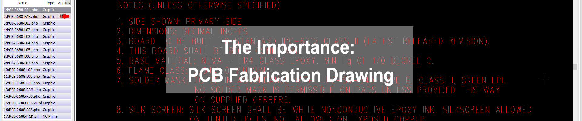
What is a PCB Fabrication Drawing
PCB Fabrication Drawing is a specific document present the critical information related PCB manufacturing. Generally, it includes some basic fabrication notes (such as PCB thickness, surface finishing, solder mask color, silkscreen color, impedance details, conformal coating, peel-able mask, critical tolerance, etc), drill table, scaled drawing, stack-up drawing, assembly array drawing, and other special notes if any. It is generally released with PCB Gerber file by a separate file.
Unlike PCB assembly, bare printed circuit board is a typical of customized product that take time to design before releasing it to PCB manufacturer. The more complex a circuit board is, the more detail manufacturing specification is a must. A professional circuit board manufacturer always prefer a detailed fabrication drawing to a common and default specification. From a fabrication drawing a PCB supplier will find answers to some manufacturing questions.
Why Do You Deed a PCB Fabrication Drawing
The purpose of a PCB fabrication drawing is to present what the final finished circuit board will exactly be. Whether there is one specification that can fit all PCBs fabrication? The answer is No., as each circuit board has unique manufacturing and quality requirement. These must be defined by end-users (or PCB designer) based on their actual product application field. The fabrication drawing is also for PCB fabrication house used to perform necessary verification, to identify any inconsistencies between CAD data and specifications, such as hole quantities, the holes non-plated and plated properties, etc. Besides, the fabrication drawing is used for final qualification checking, allowing quality inspector to ensure the manufactured PCBs meet the specifications presented on the drawing.
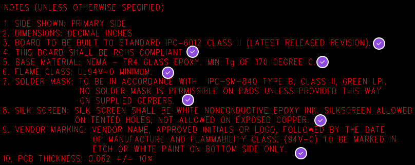
Fabrication Notes
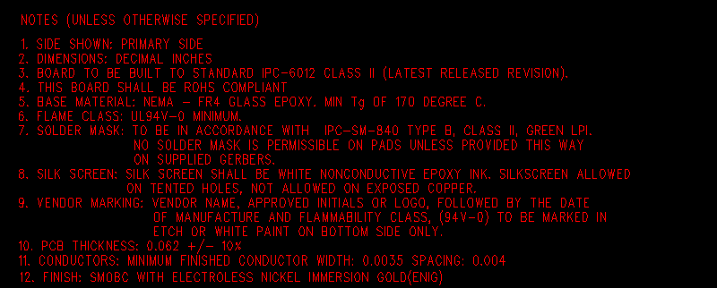
The fabrication notes generally listed by several items, which referred as a tooling for circuit board design engineers to specify the cosmetics, physicals, and function of the final PCB. Additionally, the fabrication notes are communication between the PCB designer and circuit board fabricate house. PCB factory can interpret the notes into manufacturing instructions to control the quality of the PCB. And, a complete PCB fabrication drawing should also provide accurate specifications for the finished circuit board. In order to achieve the optimal electronic and mechanical performance of the manufactured circuit board, a circuit board design engineer should be very familiar with the related IPC specifications. IPC-6012, the qualification and performance specification for rigid printed boards; which provides PCB design engineers multiple options to specify on the finished PCB.
Specify Quality Standard of the PCB
For example, when it comes to specify the base material, the PCB designer should specifically specify the The glass transition temperature (Tg) of the base substrates. This is vital to ensure the PCB can withstand thermal chock and the amount of heat cycles during PCB assembly process. This has been specifically defined by IPC 4101. For example, IPC-4101/126 specifically specify the baster material must meet Tg (min) 170 and Td (min) 340. For some special industries’ circuit boards, such as military, aerospace, the PCB designers should have specific knowledge of the material selection criteria. Another method to control PCB quality, and cost, is to specify a quality standard of the circuit board. For example, IPC-6012 Class 3 may be required for a high reliability circuit board, but the PCB manufactured by class 2 and 1 will have less quality requirements and inspection points. Accordingly, IPC class 3 raise up the PCB manufacturing cost, but Class 1 and Class 2 have lower overall cost. IPC-6012 Class 2 is a general standard commonly used in the PCB industry, but some IPC class 3 points separately required, like holes copper plating thickness.
Specify Quality Standard of the PCB
When specifying surface finishing, design engineers can also specify surface finish’s durability per IPC 6012 and Industry Standard -003 (J-STD-003).
It is very important to have your PCB fabrication notes presented as simple and as clearly as possible. Vague or open-to-interpretation notes can lead to manufacturing delays, misunderstanding or errors, resulting in unnecessary costs and lost time.

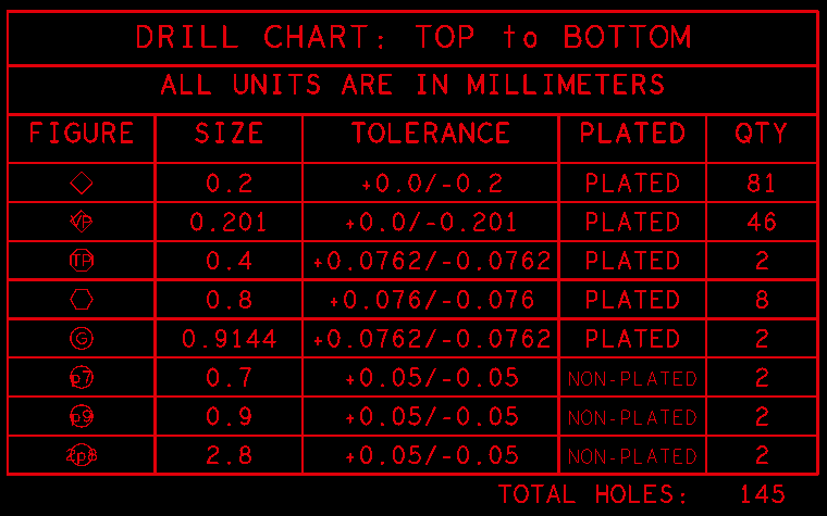
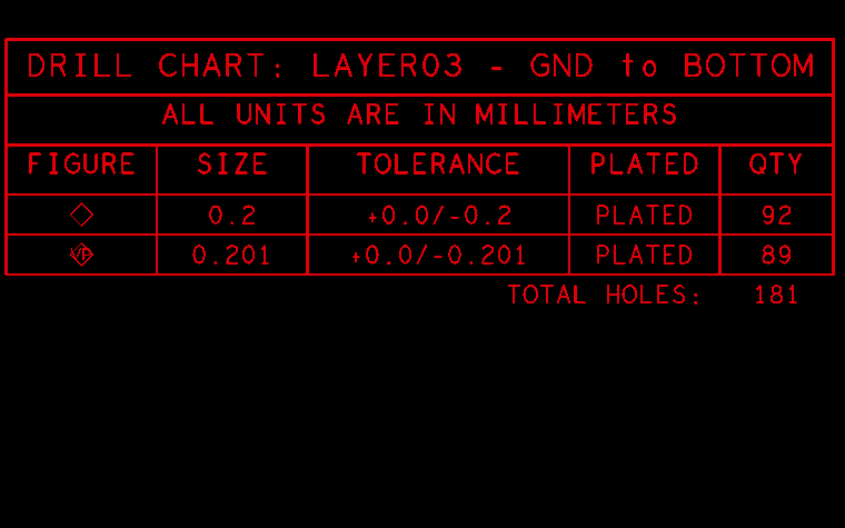
Drill Table
The drill table related the holes and slots drilled (or routed) on the PCB, which is another critical element of the fabrication drawing used for design verification. It defined all the holes to be drilled into the PCB, including the sizes, quantities, tolerances, plated or non-plated, and symbols that match the drill drawing artwork. Each symbol indicate the placement of each hole on the circuit board. PCB design engineers can also add extra information, such as for blind and buried vias for HDI circuit board, specific tolerances for press-fit holes, etc, to minimize questions from the CAD engineers of PCB factory. Sometimes CAD systems are not 100% correct and generate mistakes that are out of our control or unknown to us, the double work on fabrication drawing provides additional assurance.
Scaled Drawing
The mechanical drawing is also an important part of fabrication drawing. This drawing should provide some critical dimensions including the accurate outline of the PCB. Also some extra information can be specified on the mechanical drawing, for example, edge plating zones, the details of countersink and counterbore hole, back drilled holes, the zones of copper coins, etc. In addition to the mechanical dimensions, a good mechanical drawing will include an origin point for the PCB manufacturer to use it as global dimensions verification.
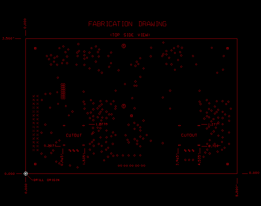
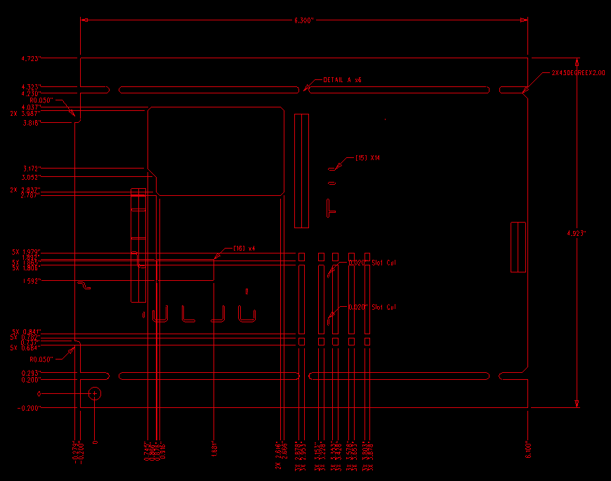
A professional PCB manufacturer will be always firstly check the related dimensions on mechanical drawing. Usually, designer’s CAD system was incorrectly configured for Gerber data output, sometimes the physical layers scaled differently than the drill files. Therefore the PCB dimensions can help to figure out the issue quickly, this is very useful.
However, adding too many dimensions on the drawing can make it unreadable and complexity the work. It probably take extra confusion to factory engineers when too many dimensions and angles included on the drawing. Therefore it’s best to include only overall and some critical dimensions.
Stack-up Drawing
A PCB stack-up drawing sequentially shows the circuit layer construction of a multi-layer PCB. This is not always needed in every PCB manufacturing document package, some special designs require specific information. For a single or two-layer PCB, PCB designer only need to specify the copper thickness, the finished board thickness and tolerance in the fabrication notes. However, some PCB designs will need a stack-up drawing with more detailed specifications.
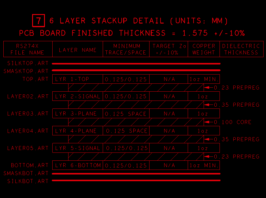
Some senior PCB designers regularly specify the layer arrangement in the PCB packages, but some other designers always fail to be this simple work.
PCB designers can specify finished copper thicknesses for each circuit layer, core thickness and dielectric thickness between layers. These are great information as long as they are presented accurately. However, some stack-ups present these thickness mismatched final PCB thickness, then this will raise up a question flag from PCB manufacturer as engineering questions asking for confirmation. This resulting in placing the board production on hold in engineering, and lead to add more lead time even extra cost to the PCB.
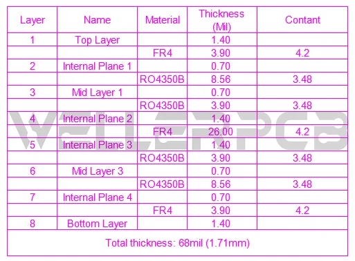
Specify Material Type in the Stack-up Drawing
A PCB design with bind, buried or back drilled holes may have multiple drill sequences. A drawing presenting all the drill sequences will have the supplier thoroughly know the number of laminate pressing and drill cycles before final inspection, avoiding the guesswork. Although a professional PCB CAM engineer can identify each drill segment from the PCB artwork, an educated guess is still a guess and consuming much time.
A complete stack-up should also present the base material type and the dielectric thickness between layers. Usually this information is necessary for the circuit board with controlled impedance requirements. The specific material type and dielectric thickness can help control impedance track, and with careful manufacturing’s optimizing and compensation, PCB production engineers can mostly minimize Electromagnetic Interference (EMI) and crosstalk through strategic reference plane placement.
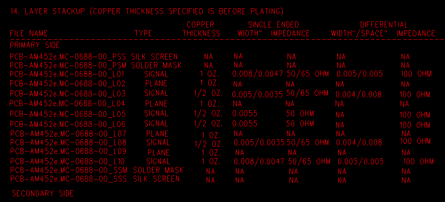
General Stack-up Drawing
The stack-up drawing is a great way to specify controlled impedance requirements and details. The best impedance trace details are placed in a specific table, identifying the impedance traces on each layer. Also the table should include impedance track width, space for structures, target impedance value for each (pair) traces, and the layers each trace will reference.
Some special application PCBs have thermal management specifications like copper coin technology or Insulated Metal Substrate (IMS). Copper coins and metal substrates come in multiple shapes and sizes. The stack-up drawing is a good option to show PCB manufacturer about the thickness and shape of the coins and the details of the IMS technology, for example, the thickness of thermal dielectric and metal substrates.
What is Controlled Impedance for a PCB?
A good manufacturing stack-up usually including layer arrangements, copper thicknesses, drill sequences, and dielectric thickness ensuring that the finished PCBs meet controlled impedance requirements. Contact us freely for our PCB design guidelines for Stack-ups and impedance to get your PCB design right from the start.
PCB Stack-up and impedance drawing
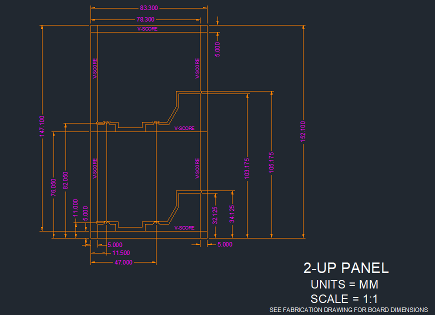
PCB Array Drawing
A array drawing is a scaled drawing presenting the number of PCBs in each array. It should remark dimension measurements and have accurate spacing between each circuit board. At most cases the rails is necessary to array for convenience of PCB assembly. The rails of an array should have at least three fiducials and four tooling holes placed on. Fiducials are used by SMT machines to maintain accuracy through PCB assembly, the tooling holes is used for tightly hold the boards during some PCB production process such as electrical testing, outline or profile routing. When the circuit board design has uneven distribution of circuit traces and copper planes, then the dummy PAD (or thieving) is needed to ensure more uniform plating across the panel, while the rails are a good place to add it without affecting the circuit board.
Reversions updating is a common work in electronics design field. An updated fabrication drawing can save engineering time of design for manufacturing. Most PCB factory’s engineers and buyers do not like much time spent in front-end engineering. A good updated fab drawing will speed up the engineering review and have the PCB manufactured at a better lead time. Additionally, try to make your update as simple and thorough as possible. The redundant information. Too much redundant information could increases the risk of missing something during revision, and leading to additional questions and longer lead times.
A complete PCB fabrication drawing will take a great feeling to PCB manufacturing house. The drawing should be very clear and concise with containing all necessary information. If the details or notes are scattered, it’s better to revise it as simple and clear, no confusion. PCB production is a type of custom manufacturing service. The experienced manufacturer well know how to manufacture the board at high quality and high reliability, but they may not have the experience in manufacturing particular design. This may require some extra questions and communications, the purpose of the PCB fabrication drawing is to minimize thoroughly eliminate these questions. More or less optimizing this part of the design is a time-consuming work, but absolutely it is worth to do it for a better quality, cost, and lead times.