

Typical 10 Layer PCB Stack-up Design Guidelines
If you are starting a 10L rigid PCB design, and a standard stack-up can meet your electronic device operating performances, you can check our online standard 10L PCB stack-up, which may offer you best reference in time and cost saved.
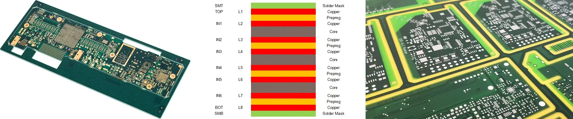
Typical 8 Layer PCB Stack-up Design Guidelines
Our standard 8L PCB stack-up design options are suitable for most electronics design with upon global considerations of durable reliability, operation performance, economic cost and more available to PCB manufacturing process.
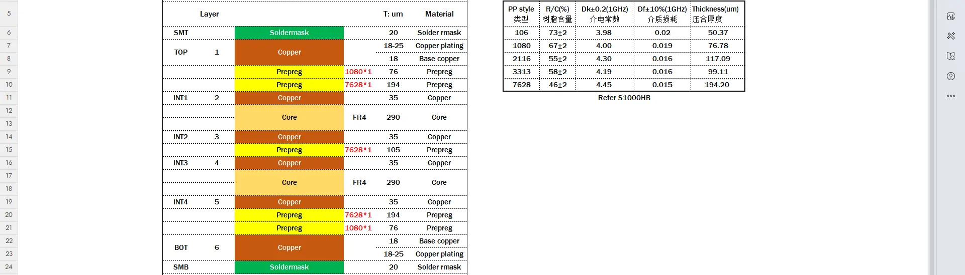
Typical 6 Layer PCB Stack-up Design Guidelines
Our standard 6L PCB stack-up design options are suitable for most electronics design with upon global considerations of durable reliability, operation performance, economic cost and more available to PCB manufacturing process
RF and Microwave Printed Circuit Boards
RF and microwave printed circuit boards are more and more applied to some advanced remote communication systems such as aerospace, radars, wireless communications, etc.
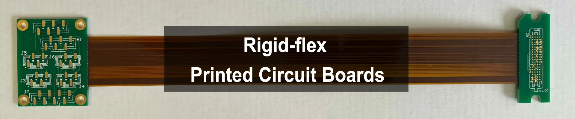
Rigid-flex Printed Circuit Boards
With rapidly developing and upgrading in electronics devices, more and more rigid-flex printed circuit boards are applied to new generation electronics devices such as mobile phones,computers, advanced displays, medical products, etc.
How 5G Technology Can Impact The Electronics Manufacturing Industry
5G means the 5th generation mobile network. It is a new global wireless standard after 4G networks with offering higher upload and download speeds, more consistent connections, and improved capacity.
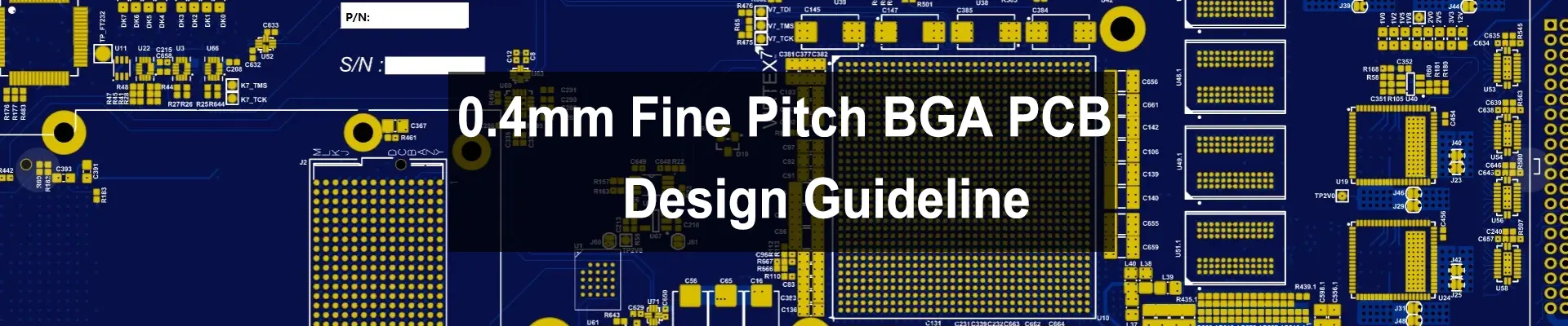
0.4mm Fine Pitch BGA PCB Design Guidelines
Nowadays, more and more precise electronic components are widely used in some advanced electronics devices, such as fine pitch FPGA component from Xilinx. But accordingly this take extra challenges to PCB designer and PCB manufacturing’s capability when the design has many limits in spacing of tracks, plated holes, electronics performance, etc.
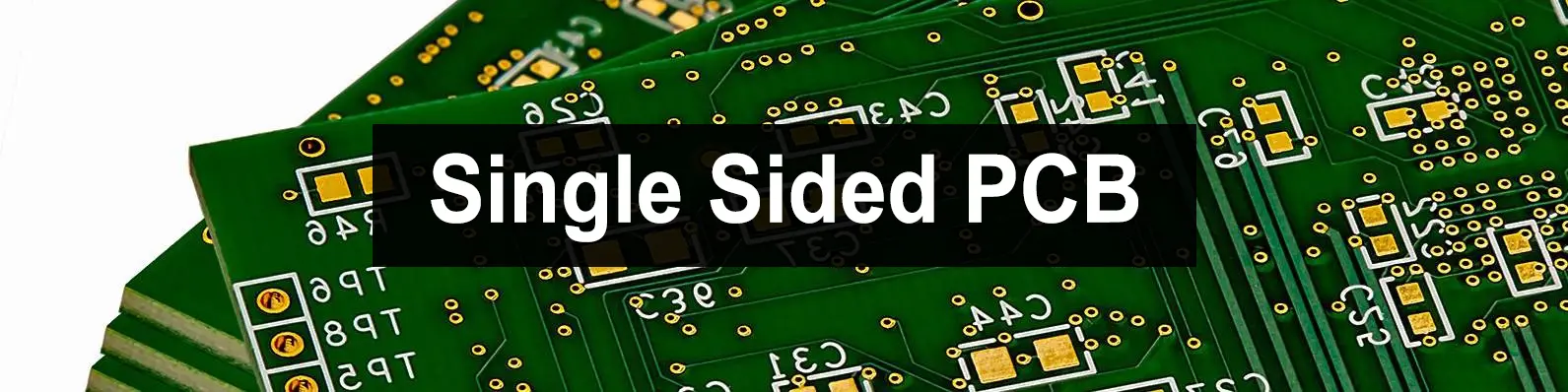
Single Sided Printed Circuit Boards
Single sided PCB, as known as one layer circuit board, which is a printed circuit board with only one copper layer of conductive material above the substrate. And also the electronic components mounted on one side of the board and the conductive track connected on the other side. So, it is called the one layer printed circuit board,..