What is a PCB stack-up?
A PCB stack-up shows the circuit layer construction of a multilayer printed circuit board board in sequential order. It specifies vital information including: material type (FR4 with specific Tg value), material thickness, copper weights, dielectric thickness… A good design stack-up along with advanced PCB manufacturing will have positive impact on the electric performance of your circuit board.

The Importance of PCB Stack-Up
At most time the importance PCB stack-ups is overlooked by PCB designer and PCB manufacturer. Many times, the stack-up in multi-layer PCB Gerber files sent for manufacturing are missing some significant data, most of them just mentioned the copper thickness and overall PCB thickness, no specific thickness in dielectrics or stack-up drawing details.
But no matter the project, small or big, trivial or complex, prototypes or mass production, designing a good stack-up definition can greatly improve long-term reliability and best performance, reduce production costs, and allow for a smoother transition to manufacturing.
Stack-Up Details
A typical PCB stack-up will specifically define circuit sequence, copper thicknesses & insulating substrate types, and final finished PCB thickness with accepted tolerance, such as 1.60+/-0.16mm. PCB circuit layers can contain a range of copper thicknesses, from 1/3 oz to 6 oz or more. This can be easily understood since that is how signals and power are operated – the primary purpose of a PCB. But depending on the exact design requirements, the type of a PCB (hybrid, high frequency, high heat, high speed, etc.) may vary quite a bit and, as a result, the stack-up will look not same too.
As simple as it is, A very simple single layer PCB just contains substrate, copper, soldermask, and a silkscreen layer for labeling if any. A multi-layer PCB will contain multiple circuit layers of these materials plus prepreg and core. The prepreg is a semi-cured dielectric material (such as fiberglass impregnated with resin) that bonds two cores or a core and a copper foil (even in two copper foil for some HDI PCB stack-up) in a PCB, while the core consists of a fully cured material (like FR4) with the copper foil laminated to each side.
With multi-layer constructed printed circuit boards, especially high-layer ones with advanced materials and complex requirements, it is absolutely critical to carefully plan and technologically consider the stack-up.
PCB Stack-up Examples
Multi-layered PCB have outstanding advantages of better energy distribution, cross-interference reduction, while eliminating electromagnetic interference and supporting high-speed signal transfer. These type of circuit boards also help minimize external noise vulnerability, radiation, and decrease impedance/crosstalk problems.
Advanced Technologies
There are also more complexity PCBs that we specialize in manufacturing. All of these advanced PCB designs have special stack-up considerations.
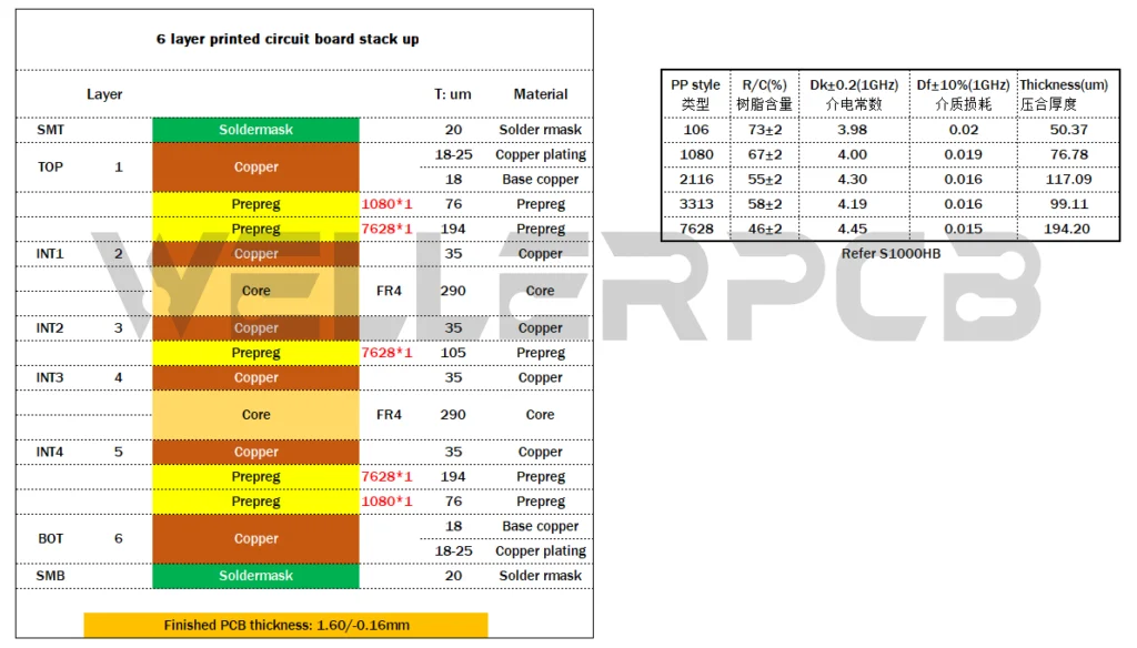
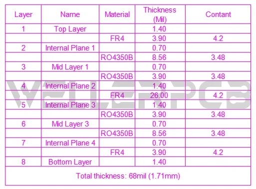
6 Layer Rigid PCB Stack-Up
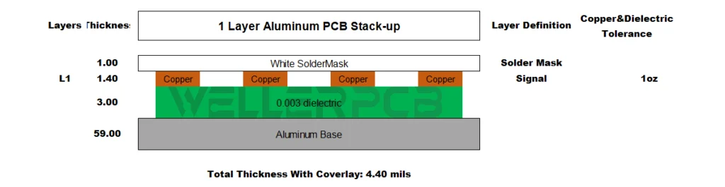
Metal Core PCB Stack-Up
Metal Core printed circuit boards (MCPCBs) commonly used for high-current LEDs and other high power transmission applications.
The metal core (copper or aluminum) takes up most of the board thickness and provides two purposes. The first is to help dissipate heat away from the junctions of the ICs or high power components during operation. The second is to provide a flat, conductive surface on the bottom that can be mounted to external heat-sinks.
High Density Interconnect (HDI) PCB Stack-Up
Ultra HDI (High Density Interconnect) PCBs containing blind, buried, and microvias for ultra compact digital designs. Typically these PCB designs contain a very high performance processor with very high speed data buses including memory and connections to off-board serial and parallel peripherals like PCI interfacing devices. With very small size, non-standard via holes, extremely complex impedance-controlled traces, and high density footprints with tight clearances and solder-mask specifications, no surprising that these type of boards can contain many layers.
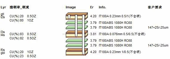
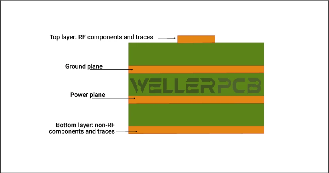
Remote Frequency (RF) PCB Stack-Up
Remote frequency (RF) PCBs are widely used for applications that require signal flow rates and frequency ranges up to 100 GHz, with the devices such as wireless transmission systems, smartphones, radar, sensors, and security systems.
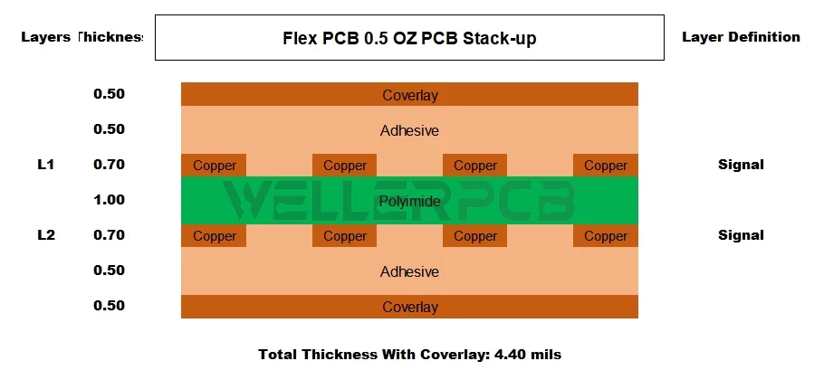
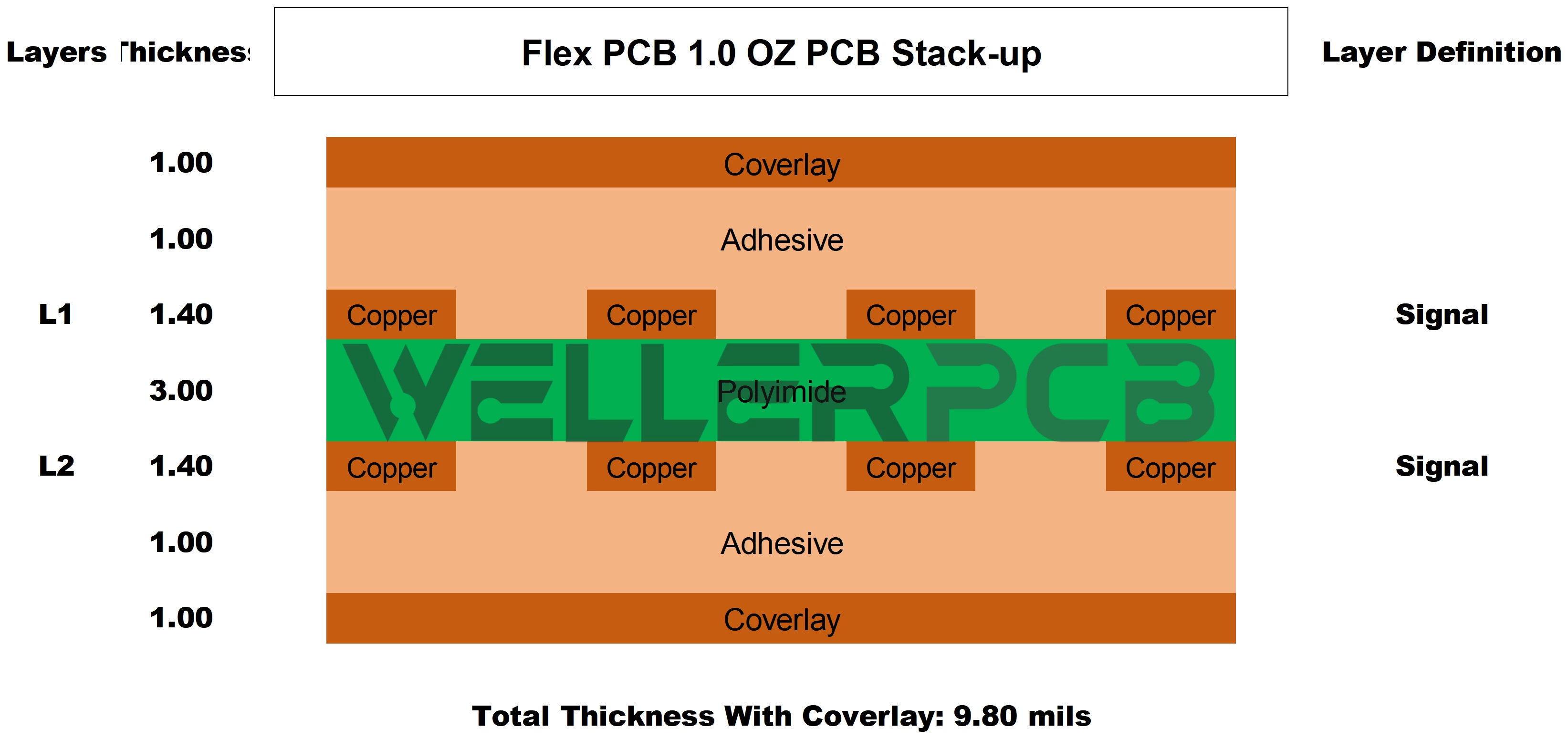
Flex & Rigid-Flex PCB Stack-Up
Flex (also called FPC) and Rigid-Flex printed circuit boards are widely used for small, flexible applications such as wearable and hand-held devices. These type of “circuit boards” may be just flex or can be a mix of rigid and flex boards to make up a single PCB assembly that can bend and fold. Flex PCB are made up of a flexible polymer, copper layer (1, 2, or even more!) and an overlay, and can utilize planes, traces, and vias just like any other standard rigid circuit boards.
Stack-Up Requirements
Many things determine the stack-up requirements for a PCB, but the critical factors are:
Copper Foil Construction vs. Cap Construction Stack-up
PCB lamination is the stage of PCB manufacturing where the inner layers, prepreg, core, and copper foil are composite into a multi-layered stack that is laminated together with heating, pressure, and cooling to complete the multi-layer PCB.
There are two ways to laminate a multi-layer PCB – foil and cap.
Foil construction/lamination is the preferred and the recommended option than cap construction.
In most cases, copper foil construction is better for layer to layer and drilling registration with easier manufacture-ability at a better yield. The cost is relatively lower since it requires less core laminate material and provides higher yields.
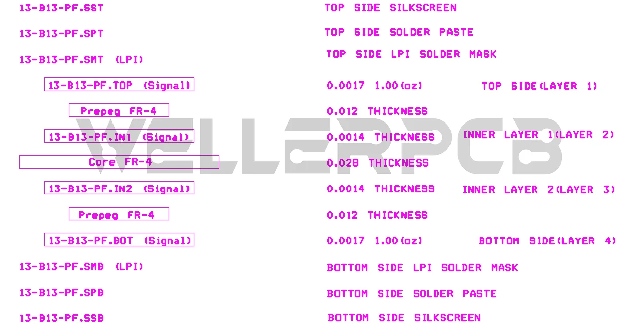
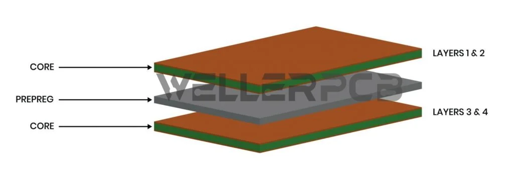
In a copper foil construction, the prepreg is locating between the outer copper layers. For example, on a 4 layer circuit board board,it is between layers 1 & 2 at the top as well as in between layers 3 & 4 at the bottom. A continuous copper foil sheet makes up the outside of the PCB manufacturing panel.
The stack-up below shows the foil construction of a 4 layer circuit board, consisting of the following layers from top to bottom:
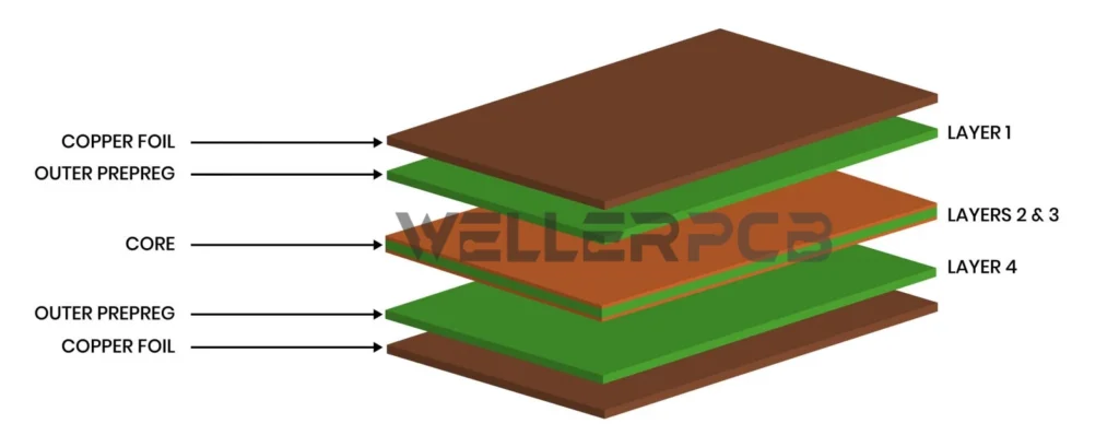
Note: The prepreg and copper layers are presented as 2 different colors in the stack-up above to illustrate how it will be manufactured. In reality production, they are the same color as usually they are the same material.
A cap construction has the two outer copper layers on pieces of pre-copper cladded laminate also called core material to make up the cap layers.
The above 4 layer PCB stack-up would have the outer copper layers starting with core laminate with a single prepreg layer in between them as a role of boning and insulating.
Unless there is no choice, cap construction is not recommended in modern PCB manufacturing process. This method is only suitable when requirements call for hybrid PCB design with specialty laminates or some blind via holes when regular drilling methods are not available, like laser drilling.
The below stack-up illustrates the cap construction stack-up of a 4 common layer board, consisting of the following layers from top to bottom:
PCB Component Density (number of layers & spacing)
Overall PCB board density is the most common driving factor; some complexity design like high pin-count processors or memory in Ball Grid Array (BGA) footprints. Depending on the pitch and pin-out pattern, in most cases, it have to take several extra layers just to distribute the signals from the inner sections of the footprint.
Component Types and Interfaces (analog, digital, mixed signal, high-speed)
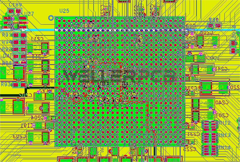
Even though it saves a lot of board spacing, electronic designing with BGA components is sometimes not ideal as it adds more complexity (and rise the manufacturing cost) during PCB production; in addition to taking much difficult to rework when needed. The picture below shows a 676 pin BGA component that requires several circuit layers for routing to each pad.
PCB Type & Application
The system thermal management is another critical driver of stack-up requirements. For PCB that contain many power components or manage high current traces, it may require more layers for power planes/nets and lots of copper to help keep resistance down (lower inductance resistance drop) or to dissipate power from thermal junctions of components.
Learn more about PCB material selections.
Some RF components (like RF switches or RF cables) require several paths (planes) to help with power dissipation and improve grounding. Analog intensive PCB design also may require several ground planes to optimize Signal-to-Noise Ratio (SNR) and reduce Electromagnetic Interference (EMI). And circuit boards with sensitive digital domains like Ethernet, USB, DDR, PCI, etc. may also have dedicated internal layers with additional grounding planes.
The image below shows a Stack-up design in PCB production process consisting of 4 layers and blind/buried vias.
Mechanical Requirements
There are critical mechanical reasons for having PCB boards limited at certain thicknesses.
For example, a mechanical engineer may propose 2 layers for a single-sided layer board to help provide additional support for through-hole components. Or perhaps a certain configuration requires a circuit board thickness have to be 0.031” (as compared to the standard thickness 0.062”) to help reduce a little bit of height in a stack-up. Though be wary of making your PCB thickness too thin and keep bow/twist in mind, as it can easily be impacted from vibration and deflection or warping.
Some RF components (like RF switches or RF cables) require several paths (planes) to help with power dissipation and improve grounding. Analog intensive PCB design also may require several ground planes to optimize Signal-to-Noise Ratio (SNR) and reduce Electromagnetic Interference (EMI). And circuit boards with sensitive digital domains like Ethernet, USB, DDR, PCI, etc. may also have dedicated internal layers with additional grounding planes.
But mechanical requirements are not the only factor determining the thickness of circuit board. Normally, PCB manufacturers will have capability limits on how many maximum layers (depending on their copper pours) they can design and manufacture in a given thickness. For PCBs containing 4 layers or less, the standard thickness is 0.062” and it’s typically the economic cost option. Along with layer count increasing, the minimum thickness will increase as well. For example, you might be able to have 8 layers PCB with 0.062” thickness and 1oz copper on each layer, but if the requirements asked for 0.031”, there wouldn’t be enough dielectric material in between layers and the PCB manufacturer will reject the design.
Keep checking with your PCB manufacturer on capabilities before getting too far in the PCB layout to make sure there aren’t limits in terms of design rules and stack-up. A professional PCB manufacturer will typically recommend what’s best and present options that balance cost, lead-time/availability, reliability, and performance.
Sometimes the PCB designer may require specific materials but depending on availability and what’s in stock, the PCB fabricator might suggest a mixture or propose a stack-up that meets a tighter timeline.
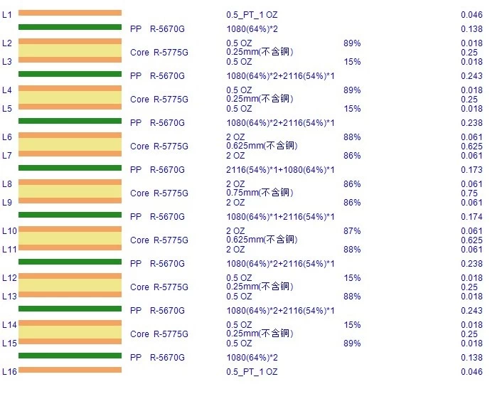
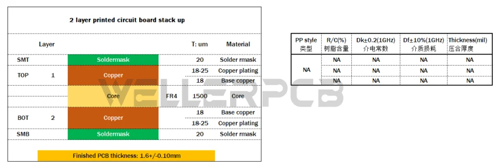
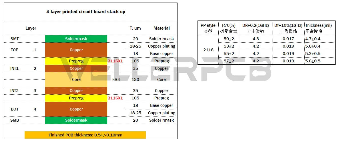
Standard Multi-layer PCB Stack-up Design Guidelines
When you start a new PCB design which required a specific stack up construction, below multiple options would be a good reference to your global consideration of cost, reliability, and performance.
Ready to discuss a PCB project?
Contact us WELLER at any time to find out how to optimize your stack-up and find that balance between cost, availability, lead-time, reliability, and performance.