

The Essential Guide to PCB Gold Fingers: Design, Manufacturing, and Applications
Printed Circuit Board (PCB) gold fingers are more than just shiny connectors – they are precision-engineered components critical to ensuring reliable electrical
Multi-layer PCB Stack-up Design Guideline
The PCB stack-up mostly determine the operating performance of an electronic devices. Therefore, it is critical to have an outstanding stack-up design for a multi-layer circuit board. This article presents some specific reference to PCB designer.
Top 10 DFM Issues that Affecting PCB Manufacturing
PCB designers have to meet various requirements and expectations. The areas they consider are electrical, functional, and mechanical. They also need to deliver
Flex Circuit Stiffeners Design Guidelines
Stiffeners is a typical necessity to a flex circuit board, the flex PCB with stiffeners designed can ensure a best PCB assembly quality. And it will also take extra reliability and durability to your final electronics products.
Advanced Plastic Injection Molding Solution To Electronics Assembly
Mold injection is an essential process to the full electronics manufacturing and box-building assembly provider. WELLER is one stop solution provider to global
Solutions to PCB Bow and Twist
Bow and twist on a bare printed circuit board are two types of deformations that can occur during and after the PCB manufacturing process.
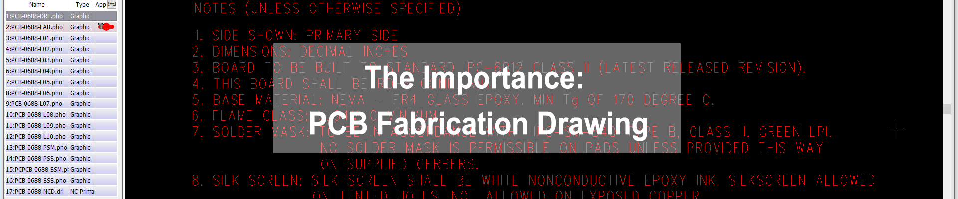
The Importance of PCB Fabrication Drawing
PCB Fabrication Drawing is a specific document present the critical information related PCB manufacturing. Generally, it includes some basic fabrication notes (
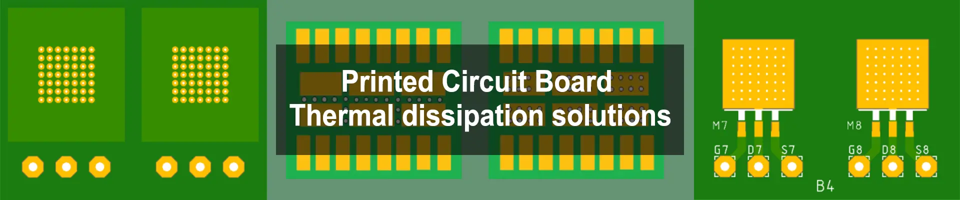
Printed Circuit Board thermal dissipation solutions
Today, with the increasing precision and powerful functionality of electronic devices, the thermal management is becoming more and more important, which normal