Introduction
PCB stack-up is an important factor in determinate the EMC (Electron-Magnetic compatibility) of an electronic product. When we talk about the PCB stack up, we are referring a multi-layer printed circuit board. An outstanding stack-up design can be very helpful in reducing the radiation and the electromagnetic interference from loops on the PCB.
On the other hand, the good buildup can be more available for PCB production process and reducing the manufacturing cost accordingly.
Stack-up Reference for PCB Design
Below four factors are very important with respect to circuit board layer stack up considerations:
Usually not so much consideration is given except as to the number of layers. In many cases other three factors are equal of importance. Item number four is sometimes not even known by the PCB designer. In deciding on the number of layers, the following should be considered:
Often only the first item is considered. In reality all the items are of critical importance and should be considered equally. If an optimum design is to be achieved in the minimum amount of time and at the lowest cost, the last item 5 can be especially important and should not be ignored.
Multi-layer circuit boards using ground and/or power planes to provide significant reduction in radiated emission over two layer PCBs. As a rule of thumb, that is often used, is that a four-layer PCB board will produce 15 dB less radiation than a two-layer circuit board, all other factors being equal. Circuit boards containing panes are much better than these without planes for the following reasons:

Although two-layer PCB boards have been used successfully in UN-shielded enclosures at 20 to 25 MHz, these cases are the exception rather than the rule. Above about then or fifteen MHz, multi-layer boards should normally be considered.
When using multi-layer boards there are five objectives that you should try to achieve. They are:
Often we are faced with the choice between close signal/plane coupling (objective #2) and close power plane/ground plane coupling (objective #3). With normal PCB construction techniques, there is not sufficient inter-plane capacitance between the adjacent power and ground planes to provide adequate decoupling below about 500 MHz. The decoupling, therefore, will have to be take care of by other means and we should usually opt for tight coupling between the signal and the current return plane. The advantages of tight coupling tween the signal (trace) layers and the current return planes will more than outweigh the disadvantage caused by the slight loss in internal plane capacitance.
An 8 layers circuit board is the fewest number of layers that can be used to achieve all five of the above objectives. On 4 or 6 layers circuit board some of the above objectives will have to be compromised. Under these conditions you will have to determine which objectives are the most important to the design at hand.
The above paragraph should not be constructed to mean you can’t do a good EMC design on a 4L or 6L board, because you can. It only indicates that all the objectives can not be met simultaneously and some compromise will be necessary. Since all the desired EMC objectives can be met with an 8L board, there is no reason for using more than 8L other than accommodate additional signal routing layers.
Another desirable objective, from mechanical point of view, is to have the cross section of the PCB board symmetrical (or balanced) in order to prevent warping,this is also to facility in PCB board manufacturing process. For example, on an 8 layers PCB board if L2 is a plane layer, then L7 should be also a plane layer. Therefore, all the configurations presented here use symmetrical, or balanced, construction. If an unsymmetrical, or unbalanced construction is allowed additional stack-up configurations are possible.
Normal PCB Stack-up Layer Sequences Reference:
4 layer PCB stack up sequence options:
Normally, there are 3 options for 4L board stack up sequences
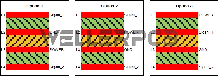
Obviously, option 3 is not so good due the the poor matching between power layer and ground plane layer.
How to select between option 1 and option 2?
Commonly, PCB designer like to choose option 1 as a 4 layers PCB stack up sequence instead of option 2. The reason is that in normal 4 layers PCB, only top layer should be components assembled, therefore option 2 is better than option 1.
But, if you need to place components both on top and bottom layers, and the need the thick dielectric thickness between power layer and ground plane layer with poor electrical matching, you should consider which layer should be considered to place small quantities of signal track. For option 1: due to there is small quantities of signal track in bottom layer, large area of copper ground can be placed there to match power layer; on the contrary, option 2 is good if most component placed on the bottom layer.
If using a symmetrical stack up; and well electrical matching between power and ground layer, option 1 is good for symmetrical features.
6 layer PCB stack up sequence options:
Normally, there are 3 options for 6L board stack up sequences
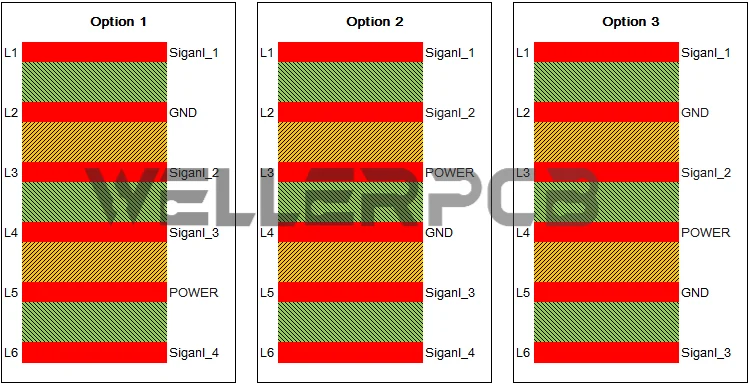
6L PCB stack up sequence options
| Option 1 | Option 2 | Option 3 |
| Designed as 4 signal layers+2 power/ground plane layer. As there are more signal layers so it is benefit to the PCB layout for components. But meantime there a some weakness in this option as below: | Easily to catch electromagnetic interference between layers Signal_1, Signal_2(Inner_1), Signal_3(Inner_4), and Signal_4(Bottom) | Compared option 1 and option 2: one signal layer deleted, one power layer added. It perfectly solved the weakness in option 1 and option 2 although one signal layer deleted: |
| ① power plane/ground plane coupling is not good due to the big distance between power layer and GND layer, | ① Good coupling between power plane/ground plane. | |
| ② Easily to catch electromagnetic interference between two signal layers inn Signal_2(Inner_2)and Signal_3(Inner_3 | ② Electromagnetic interference avoided due the power/GND plane layer following up each signal layer.. | |
| ③Signal_2(Inner_2) is next to power/GND layers (GND(Inner_1)+POWER(Inner_3)), this lead to Signal_2(Inner_2) can carry high speed signals. power/GND layers can effective have shields to Signal_2 (Inner_2) from outsource Electromagnetic interference and Signal_2(inner_2)’s Electromagnetic interference to outsource |
So, conclusion to above 3 options: option 3 is best option for 6 layers PCB stack up sequence design, which is also commonly used to 6 layer PCB stack up sequence.
From above options, more or less we have some thoughts on the design the PCB stack up sequence. But, above options can not cover all the possibilities existing in the design of a circuit boards, the priority level to different options should be considered then.
It is a pity that because the layer up sequence design is closely related to it’s exact circuit diagram, different circuit diagram determine the different feature in shield of interference, so exactly there is no fixed priority level of design for reference. But, below basic rule need to be followed:
Keep close compiling in power/GND and signal layer; and, if one layer is for high speed signals transmission, this layer must be placed between GND and power layer.
PCB stack up reference for PCB manufacturing
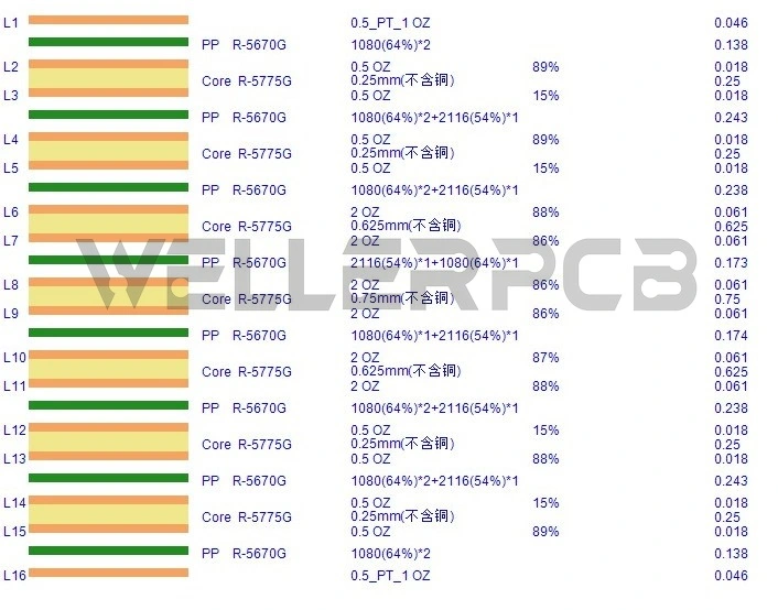
Once your PCB layer count and it’s stack sequence fixed, next step is to design PCB stack structure.
If you have assigned PCB stack up (assigned thickness of PP, core, copper) for your printed circuit boards, you need to have a through consideration when you start design your PCBs.
Otherwise, your stack up is unavailable for manufacturing process and would have your time wasted and redesign the PCB.
It is important to know the PCB manufacturing capability before starting a PCB design and it’s stack up. Below in table is some common tips about China PCB factory.
| Item | Design instructions |
|---|---|
1. Symmetrical stack-up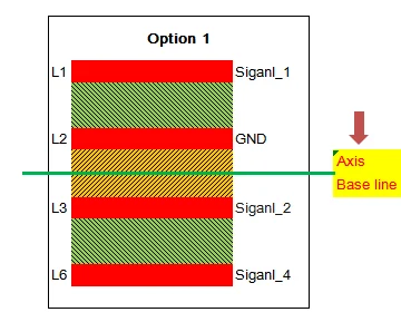 | A.draw on stack up’s axis as the base line, the structure separated by this base line must be symmetrical (core thickness, prepreg thickness,copper thickness,remaining copper, etc). B. The separated thickness splitted by base axis line should have max difference as below <1>. Core thickness difference <=0.2mm <2>. PP thickness difference <=0.2mm <3>. Copper thickness difference <=35um <4>. Remaining copper thickness difference 50% C. Any difference beyond above in item B need to discussed with PCB designer <1>. core thickness difference <=0.2mm <2>. Can bu manufactured if PCB design do not allowed to change the stack up, but the bowl and twist must be accepted as 1.0-1.5% <3>. Working panel size must be less than L<=18 inch |
| 2. Prior to use core with heavy thickness | The more heavy core thickness, the more stable manufacturing features, which could reduce the apertures risks. The features of PP should be considered to determine the core. |
3. Hate to use core + core structure.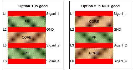 | One more core used, means the more manufacturing process challenge take. <1>. Prior to use heavy thickness core or the heave thickness of PP for some critical layers instead of directly replacing by core. <2>. Prior to use “Core+PP” instead of “core + core”. |
| 4. Prior to us prepreg 7628 | <1>. The priority level of prepreg: 7628->2116->3313->1080->106 (excluding special case) <2>. Below stack-up could be optimized as priority as prepreg 7628 (excluding special case): “21162+1080”==>”7628+2116” “33132+1080”==>”7628+3313” “10802+2116”==>”7628+1080” “10802+3313”==>”7628+1080” “2116+3313+1080”==>”7628+3313” |
5. The light thickness of prepreg placed towards to sequence of the out-layer instead of inner layer.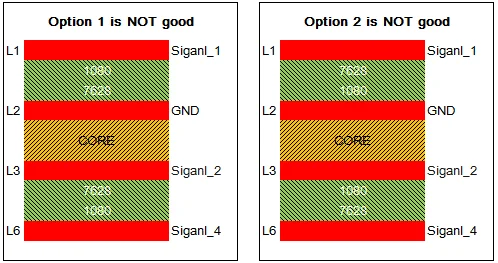 | The purpose is: <1>. Avoid the defects of woven of Prepreg, so the lighter thickness PP should be placed at out-layer. For example: 7628+1080; But, no any limitation if >= 2 PCS of 7628 required. |
6. 1080 is not allowed to placed on both out layers (top and bottom).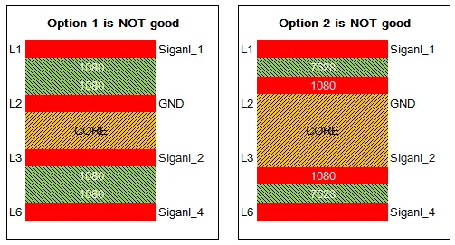 | <1>. This will take extra difficulty once rework need to be done. Not good for 10802,10803,1080*4, etc. <2>. To facility to the potential rework of production, prior to use 1pcs below PP at least for outlayer’s dielectric: 7628, 2116, 3113, |
| 7. The quantity of prepreg <=3 | Excluding heavy copper thickness PCB board such as 3oz, 4oz, etc. |
8. Prior to use “Core+PP” instead of “Copper+PP” for high frequency PCB.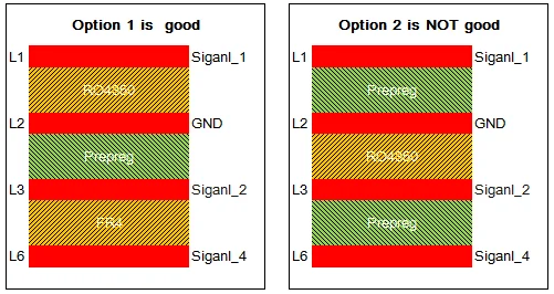 | “Copper+PP” structure for high frequency PCB is easy to take problem of out copper layer’s de-lamination. |
When all your circuit board designs finished you can release your files to your PCB fabrication house to get a quote. If you do not have an existing PCB manufacturing partner, it will be very easy to find some ones from internet by search key words PCB China, PCB China online, etc.
At WELLER, we have a professional team to support our customers behind their high technology PCB’s fabrication, we can provide manufacturing DFM support from starting of your design.
Standard 4 layer PCB stackup design options
Standard 6 layer pcb stackup design options
Standard 8 layer PCB stackup design options
Standard 10 layer PCB stackup design options
Standard 12 layer PCB stackup design options
Standard 14 layer PCB stackup design options