Home » PCB Assembly » Die Bonding and Wiring Bonding
PCB ASSEMBLY
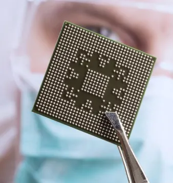
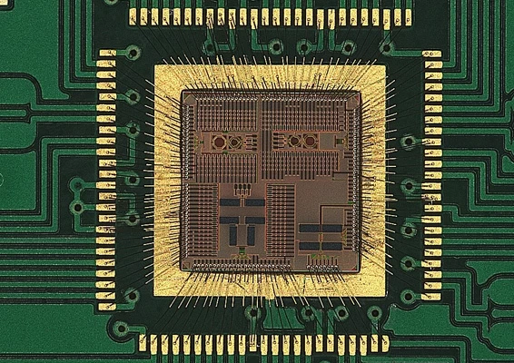
Die bonding and wire bonding are two critical semiconductor assembly processes used to create electrical interconnections within integrated circuit (IC) packages.
Bonding is a prevalent technique used to create interconnections through gold or aluminum wires during semiconductor device fabrication. It is commonly used to connect a chip or an integrated circuit to a package. Also it can be used to connect die to a printed circuit board or to another component. Bonding is the most widely used interconnect method in electronics due to its cost-effective and flexible interconnect technology.

Aluminum wedge bonding has the advantage of less susceptible to contamination than other forms of wire bonding. The disadvantage is that it is more likely to cause cratering where damage occurs to the semiconductor below the bond pad.
It is also called aluminum wedge wiring bonding, usually it forms the wire bonds at a room temperature using pressure and ultrasonic energy. It involves using aluminium bond wire to bond to aluminium (Al) or gold (Au) bond pads. Typically it is often used with aluminium bond wire to connect aluminum or god bond PADs. The formation of aluminum bonds is from force and ultrasonic, so the bonding surface does not need to be heated to 150°C or even anything above room temperature. The creation of an aluminum wire bond consists of two contacting points and a specific loop shape. During the contacting steps for the wire, the only factors needed for the bonding are force and ultrasonic energy, as the surface does not need to be heated.
Aluminum wire provides a strong electrical path for interconnections between components in an assembly also has some outstanding advantages. Bonding by this method is a good option when the interconnections to be formed on temperature-sensitive assemblies where the materials cannot withstand the high temperatures. For the bonding on the aluminum surfaces with hermetically sealed packages, aluminum wire is much better than gold wire, as the temperatures needed for hermetic sealing can break the integrity of Au on Al bonds.
Both aluminum wire and gold wire are two main material types for wire bonding. Other materials such as some alloys have also been used in some specific wire bonding applications for their unique properties. The essential aspect to a successful wire bonding is the ability to have the optimal frequency, force, and temperature for any given material.

086 (0755) 2828 2776
Don’t hesitate, contact us to start discussing your projects. We prioritize your inquiries and aim to respond within 12 hours.
Gold wire bonding is the process with combination of pressure, temperature and ultrasonic energy, by which gold wire is attached to two points in an assembly to form an interconnection or an electrically conductive path. Force, heat, and ultrasonics, are all joined to form the attachment points for the gold wire.

This process involved two stages: the fist stage is to create the attachment point begins with the formation of a gold ball at the tip of the wire bond tool, the capillary; the second stage is to have this ball pressed on the heated assembly surface while applying both an application-specific amount of force and a frequency of 60kHz – 152kHz of ultrasonic motion with the tool.
Once the first bonding has been done, the gold wire will be operated though a tightly controlled manner to form the appropriate loop shape for the assembly’s geometry. The second bonding, often called as stitching, is then attached on the other surface by pressing the wire down and using a clamp to tear the wire at the bond.
Gold wire bonding offers an interconnection method within semi-conductor packages which is highly electrically conductive, nearly an order of magnitude greater than some other solderings. Additionally, gold wires have a high oxidation resistance compared to other wire materials and are softer than most, that is essential for sensitive surfaces.
The process can vary upon the needs of the assembly. With some sensitive materials, a gold ball can be attached on the second bonding area to form both a stronger bond and a “softer” bond to avoid damage to the surface of the component. With some tight spaces, a single ball can be used create a starting point for two bonds, forming a shaped of “V” bond. While a wire bond needs to be seriously robust, a ball can be attached on top of a stitch to create a security bond, improving the stability and strength of the wire.
Some variations and many different applications to wiring bonding are nearly limitless and can be done through using automated software on advanced wire bonding systems.


| Gold wire dimensions (um) | PAD size in PCB board (Min.) (um)** | Current (mA) | Die height (Max.)(um)*** |
|---|---|---|---|
| 20 | 50 | 20mA | 300 |
| 25 | 62.5 | 20mA | 300 |
**: Normally,the PAD size on the PCB board should be 2.5 or 3.0 times than gold wire dimensions. For example, 20um gold wire match PCB PAD size 20umx2.5=50um.
***: The bonding process will be out of the scope of the operating lens once the Die height is more than 300um.
The best results for you
Don’t hesitate, contact us to start discussing your projects. We prioritize your inquiries and aim to respond within 12 hours.
Ball bumping is to use a ball bonder to form bumps on a chip, and the bumps provide the necessary interconnects between chip and substrate. This is an essential process in flip-chip applications, it can be done at the assembly or wafer level, though it is most commonly performed at the wafer level.

Ball bumping has many similarities with the first step of gold wiring boding, in which a ball is formed at the capillary and is attached onto the surface with a mixture of ultrasonic, force, and heat. However, the wire do not form a loop after attaching the ball, it is just sheared off above the ball to form a planar bump on the surface of the part.
In this process, it is vital to control ball size as it determines the overall size of the bump and a reliable bonding process is the premise to ensure a consistent wire tail length before each ball formation. There will be significant variations in bump sizing once every bump is not consistently and properly well-executed.
Just right force is also critical in the bumping process as it determines the physical shape of the bump. Finally, through a precise shearing process to separate the wire from the ball is necessary to make sure forming consistent height and planar bumps.
As the ball bumping bonding process require no masks, uses existing equipment, and in many cases provides the most cost effective method for depositing bumps on chips. Therefore, A certain number of companies are using this process for full scale production. Some companies are using the process for rapid prototyping and small volume production.
1. Bumping and coining, bumping is first stage where a normal ball bond with a short ductile fracture tip protruding from the top of the ball is bonded to the device; coining is second stage operation to make sure the bump from the first stage to be coined flat.
2. The stud bumping process produces a short loop and the crescent bond is placed on the shoulder of the ball.
It is to use a wedge tool to form the stitches on both ends, instead of the use of a ball for the first bond. The bonds themselves is thin and wedge-shaped. Both gold and aluminum wire can be utilized in the wedge bonding process, but aluminum wire is commonly at ambient temperature. Both ribbon or round wire can be used for bonding in the wedge bonding process. Differ from the capillary found on a ball bonder, the wedge bonding tool required to be oriented in the direction of the bond and as a result, can rotate to bond from any angles. This allows for bonding from any and all angles for a specific assembly.

One of the outstanding advantages that wedge bonding has over wire ball bonding is the ability to make finer pitch applications due to the size of wedge bonds compared to ball bonds. The ability to use ribbon is also imperative for some assembly designs where the use of wire can not meet the electrical requirements.
Due to not requiring rotation of the tool, wire bonding is faster than wedge bonding, the capabilities of wedge bonding can be so advantageous as no need to use a wedge bonder.
With the rapid development of the electronics manufacturing field, in addition to printed circuit board assembly, more and more semiconductor packaging requires higher technical requirements and rely on advanced equipment. If you have special semiconductor packaging requirements, you can contact us at any time.

Whether you need ultrasonic wire bonding, thermocompression bonding, or advanced flip-chip solutions, WELLER provides cutting-edge technology tailored to your production demands. Partner with us to elevate your semiconductor assembly performance—contact our experts today!
We use both gold wire width size: 20um and 25um.
Sorry, we can not. We must bond the wire on the pad with specific surface finishing.