Home » PCB Fabrication » Printed Circuit Board Surface Finishing
PCB Fabrication
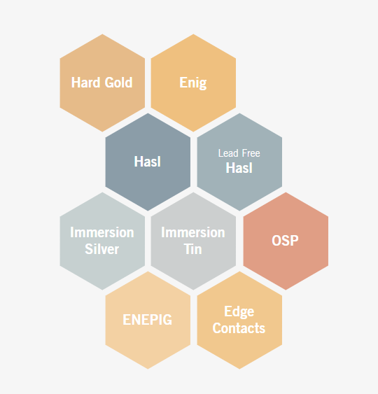
Each surface finishing has its own advantages and weakness in protecting copper circuitry from corrosion, also provides a solderable surface to the components, which one is the best to your circuit board?
A surface finish on printed circuit board can be either organic or metallic in nature. Comparing both types and all available options can quickly demonstrate the relative benefits or drawbacks.
Typically, the decisive factors when it comes to selecting the most suitable finish is the end application, the PCB assembly process and the design of the PCB itself.
Below you can find a brief summary of the most common finishes, however for further or more detailed information, please contact us and we will be more than happy to answer any of your questions.
086 (0755) 2828 2776
1. Excellent solderabilityRelatively
2. Inexpensive/Low cost
3. Allows large processing windowMultiple thermal excursions
4. Long industry experience / well known finish
5. Shelf life min. 12 months
6. Multiple thermal excursions
1. Difference in thickness / topography between large and small pads –
2. Not suited for < 20mil pitch SMD & BGA
1. Excellent solderability
2. Relatively inexpensive
3. Allows large processing window
4. Long industry experience / well known finish
5. Shelf life min. 12 months
6. Multiple thermal excursions
1. Difference in thickness / topography between large and small pads – but to a lesser degree than SnPb
2. High processing temperature – 260-270 degrees C
3. Not suited for < 20mil pitch SMD & BGA
1. Excellent flatness
2. Good for fine pitch / BGA / smaller components
3. Tried and tested process
4. Long shelf life: 6 months
5. Wire bondable
1. Expensive cost finish
2. Black pad concerns on BGA
3. Can be aggressive to soldermask – larger soldermask dam preferred
4. Avoid soldermask defined BGA’s
5. Should not plug holes on one side only
1. Very excellent flatness
2. Good for fine pitch / BGA / smaller components
3. Mid range cost for lead free finish
4. Press fit suitable finish
5. Good solderability after multiple thermal excursions
1. Very sensitive to handling – gloves must be weared
2. Tin whisker concerns
3. Aggressive to soldermask – soldermask dam shall be ≥ 5 mil
4. Baking prior to use can have a negative effect
5. Not recommended to use peelable masks
6. Should not plug holes on one side only
1. Immersion finish = excellent flatness
2. Good for fine pitch / BGA / smaller components
3. Mid range cost for lead free finish
4. Can be reworked
5. Medium shelf life if packaged well
1. Very sensitive to handling / tarnishing / cosmetic concerns – gloves must be used.
2. Special packaging required – if packaged opened and not all boards used, it must be resealed quickly.
3. Short operating window between assembly stages
4. Not recommended to use peelable masks
5. Should not plug holes from one side only
6. Reduced supply chain options to support this finish
1. Excellent flatness
2. Good for fine pitch / BGA / smaller components
3. Inexpensive / Low cost
4. Can be reworked
5. Clean, environmentally friendly process
1. Very sensitive to handling – gloves must be used and scratches avoided2. Short operating window between assembly stages.
2. Limited thermal cycles so not preferred for multiple soldering processes (>2/3).
3. Limited shelf life – not ideal for specific freight modes and long stock holding.
4. Very difficult to inspect.
5. Cleaning misprinted solderpaste can have a negative effect on the OSP coating.
6. Baking prior to use can have a negative effect.
The best results for you
Don’t hesitate, contact us to start discussing your projects. We prioritize your inquiries and aim to respond within 12 hours.
| ITEM | SURFACE FINISHES | STANDARD PRODUCTION | ADVANCED PRODUCTION |
|---|---|---|---|
| 01 | HASL ( Tin Lead Non RoHS) | 5.0 μm – 35.0 μm | |
| 02 | HASL (Lead free RoHS) | 5.0 μm – 35.0 μm | |
| 03 | Immersion Silver | 0.15 μm – 0.20 μm | |
| 04 | Electroless Nickel | 3.0 μm – 5.0 μm | |
| 05 | Immersion Gold | 0.05 μm – 0.08 μm | 0.05 μm – 0.12 μm |
| 06 | Electroless Palladuim | 0.20 μm – 0.50 μm | |
| 07 | Electrolytic Nickel | 3.0 μm – 5.0 μm | 3.0 μm – 7.0 μm |
| 08 | Electrolytic Gold | 1.5 μm – 3.0 μm | 0.5 μm – 5.0 μm |
| 09 | Pure soft Gold | 1.0 μm – 5.0 μm | |
| 10 | Organic Solderability Preservatives (OSP) | 0.10 μm – 0.20 μm |
Selecting the best PCB surface finish is critical for performance. Each PCB surface finish type – like HASL, ENIG, Immersion Silver, or OSP – offers unique advantages and disadvantages in protecting copper traces from corrosion and providing a reliable solderable surface for components. Choosing the optimal finish depends on your specific application requirements, budget, and assembly process.
Which PCB surface finish is right for your board? Contact us now to get a professional answer.
Surface finish | Cost | Shelf life (months) | Solderability | Corrosion resistance | Use cases |
|---|---|---|---|---|---|
| Organic solder ability preservative(OSP) | Very low | 6 | Excellent | Fair | Best for lead-free assembly and quick-turn boards. |
| Hot airsolder leveling (HASL) | Low | 3-6 | Good | Moderate | Works well for general-purpose & a low-cost PCB boards. |
| Immersion silver (ImAg) | Medium | 6-12 | Excellent | Fair | Great for RF and high-frequency applications. |
| Immersion tin (Imsn) | Medium | 6-12 | Good | Fair | Suitable for circuit boards with fine-pitch components and short-term storage. |
| Electroless Nickel Immersion Gold (ENIG) | High | 12+ | Excellent | Excellent | Ideal for fine-pitch BGAs and high-speed circuit boards. |
| Electroless Nickel Electroless Palladium Immersion Gold (ENEPIG) | High | 12+ | Excellent | Excellent | Perfect for HDl designs, gold wire bonding, and applications sensitive to black pad issues. |