What Is PCB Layout? Definition, Process and Key Design Elements
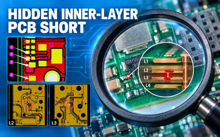
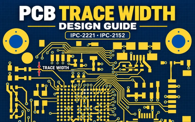
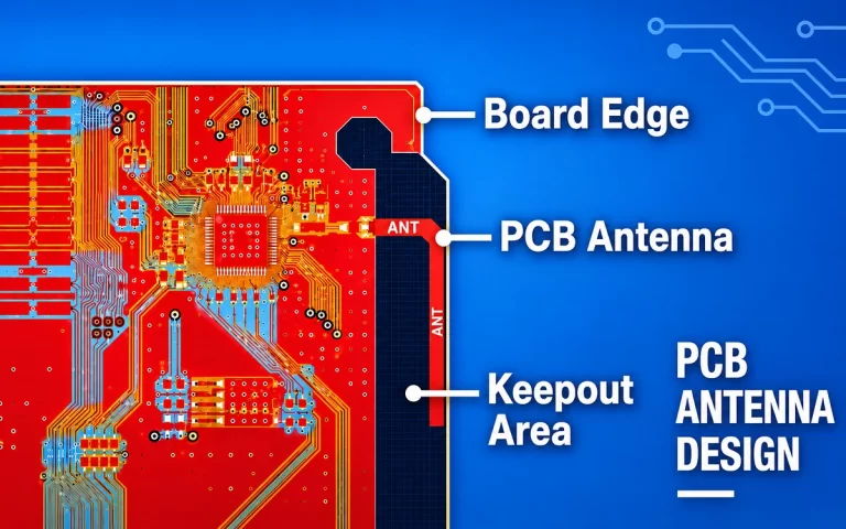
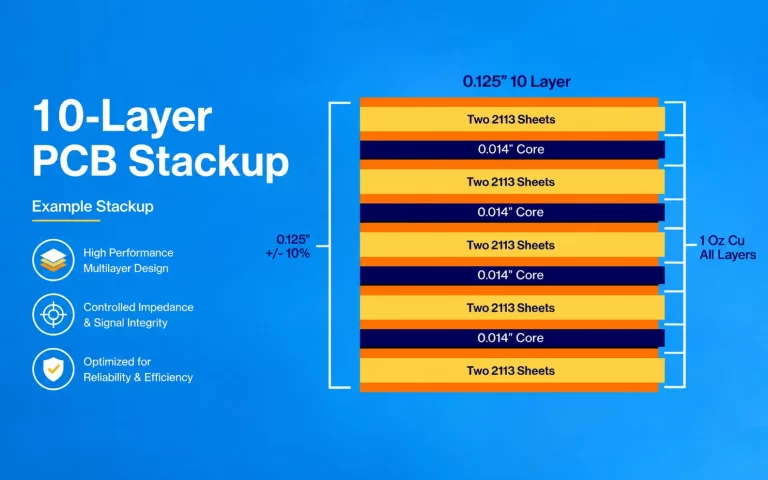
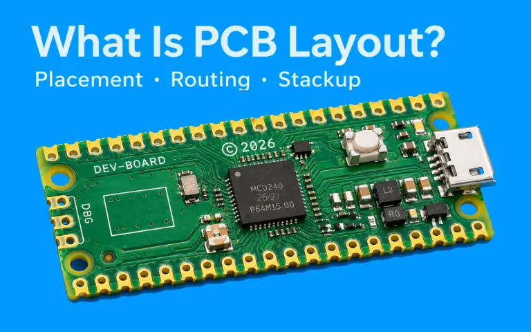
PCB layout turns a verified schematic or netlist into the physical arrangement and interconnection of a printed circuit board. It defines component footprints, placement, copper routing, vias, layer stackup, and