Table of Contents

What Is PCB Layout? Definition, Process and Key Design Elements

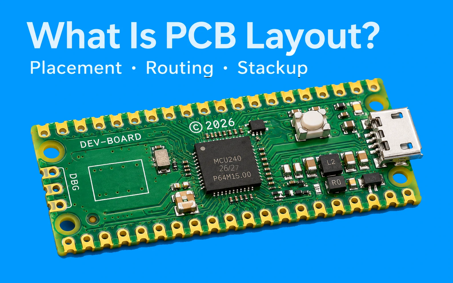
PCB layout illustration showing a green circuit board with component footprints, copper traces, and connectors.
PCB layout turns a verified schematic or netlist into the physical arrangement and interconnection of a printed circuit board. It defines component footprints, placement, copper routing, vias, layer stackup, and mechanical boundaries.
These decisions affect signal integrity, power delivery, thermal behavior, assembly, and manufacturing yield. A production-ready layout must meet electrical and mechanical requirements while staying within the fabricator’s process limits. It also requires design-rule checks, manufacturing review, and controlled release data.

What Does a PCB Layout Define?

These elements must be planned together. Component placement affects routing options, while board geometry and layer arrangement constrain how electrical connections are implemented.

Component Footprints and Placement

PCB component placement showing IC footprints, passive components, copper pads, and board layout details
PCB component footprints and placement layout
Each component needs a land pattern that matches its package dimensions, terminal geometry, and assembly method. Placement must account for connectors, mounting holes, component height, polarity, heat sources, and assembly clearance. A dimensionally incorrect footprint can cause solder defects or prevent component fit.

Copper Routing, Vias, and Stackup

Four-layer PCB stackup showing copper layers, dielectric materials, ground plane, power plane, and vias
Multilayer PCB structure and copper routing.
Traces connect pads; vias connect copper layers; planes distribute power and ground and provide signal reference paths. The stackup specifies layer order, dielectric materials and thicknesses, and copper weights. These values affect impedance, routing space, and finished thickness.

Why Do PCB Layout Decisions Matter?

Two layouts with identical schematics can behave differently because their physical current paths, parasitics, thermal paths, and manufacturing geometry differ. Check the design against the actual load, operating environment, and fabrication process.

Signal Integrity and Controlled Impedance

For fast edge rates, impedance depends on the complete transmission-line geometry rather than trace width by itself. Dielectric properties and thickness, copper thickness, and the relationship between the signal trace and its reference plane also affect the electrical characteristics.
Engineering Tip

Do not assess controlled-impedance requirements by clock frequency alone. Fast signal edge rates and interconnect length can also make impedance control necessary. Check interface specifications and driver rise times when identifying critical nets.

When a high-speed trace crosses a reference-plane gap, its high-frequency return path must find another route through the available copper and coupling paths. The resulting larger current loop can increase inductive discontinuities and radiated emissions.
Define target impedance and stackup with the fabricator before final routing. Calculate impedance from the proposed construction, confirm the released stackup, and verify it with a test coupon when specified. Generic trace-width charts cannot replace the actual stackup.

See WellerPCB’s high-speed PCB design guide for related stackup and routing considerations.

Current Capacity and Thermal Design

Power traces and planes must carry required current without exceeding permitted conductor temperature rise or voltage drop. Current capacity depends on conductor dimensions, layer location, ambient conditions, and heat transfer.

IPC-2152 provides guidance for relating conductor size, current, and temperature; final sizing must reflect product operating conditions.

For heat-producing components, review copper area, thermal vias, heatsink contact, airflow, and nearby temperature-sensitive parts together. Verify critical designs through thermal analysis or measurement on a representative assembly.

DFM, Assembly, and Reliability

Fabrication checks should cover trace width and spacing, drill size, annular ring, drill-to-copper clearance, copper-to-edge distance, solder-mask features, and layer registration. Assembly checks should cover pad geometry, component spacing, polarity, fiducials, stencil access, inspection visibility, and rework clearance.
These limits are process-dependent. Obtain the fabricator’s current rules and run DRC and DFM before release; designing at advertised minimums leaves little process margin.
WellerPCB’s SMT layout and DFM guide covers relevant assembly constraints.

Which IPC Standards Are Relevant to PCB Layout?

IPC documents address different parts of the design-to-production chain. Select standards that match board construction and product requirements, and identify the required revision and performance class in procurement documents.
Standard Primary Use Engineering Application IPC Revision Table Status
IPC-2221 Generic printed board design General design requirements Rev C, Dec. 2023
IPC-2222 Rigid organic printed boards Sectional design requirements for rigid boards Rev B, Oct. 2020
IPC-2152 Current-carrying capacity Conductor sizing and temperature-rise guidance No Longer Maintained*
IPC-7351 Rev B SMT land-pattern design Earlier land-pattern guidance No Longer Maintained*
IPC-7352 Land pattern design Component land-pattern geometry Original issue, Jul. 2023
IPC-2141 Controlled impedance and high-speed logic Reference for impedance and high-speed design No Longer Maintained*
IPC-6012 Rigid PCB performance Qualification and performance requirements Rev F, Sep. 2023
IPC-A-600 Printed-board acceptability Visual acceptance criteria Rev M, May 2025

*“No Longer Maintained” means IPC does not currently expect to revise the document. For land-pattern design, refer to IPC-7352 (July 2023).

How Is a PCB Layout Developed and Verified?

KiCad PCB Editor showing a PCB layout with component footprints, copper routing, vias, and layer controls.
PCB layout design and verification in KiCad.
A controlled workflow moves from verified inputs through placement, routing, checks, and an approved release.

1. Establish Inputs and Constraints

Review the schematic or netlist, BOM, datasheets, footprints, board outline, enclosure, and interface requirements. Record stackup, impedance, current, thermal, and fabrication constraints.

2. Place Components and Plan the Stackup

Fix mechanical interfaces first, group components by function, and reserve routing and return paths. Confirm the layer arrangement with the fabricator before controlled-impedance routing.

3. Route and Run Design Checks

Route critical signals and power paths. Run connectivity and DRC, then review mechanical fit, DFM, assembly access, and testability. Add SI, PI, or thermal analysis when required.

4. Review and Release the Data

Resolve findings, freeze the revision, and generate all release files from the same source.

Manufacturing Release Warning

Passing DRC does not guarantee manufacturing readiness. DRC checks only the rules configured in the design tool; separate reviews are needed for signal integrity, thermal performance, EMC, assembly requirements, and fabricator process limits.

WellerPCB’s PCB layout process covers requirement review, layout, DFM checks, approval, and manufacturing handoff.

What Files Should a PCB Layout Release Include?

The release package must give the fabricator and assembler consistent, revision-controlled information. The file set depends on board complexity and agreed scope.
Release Item Required Check
Fabrication Layer Data Gerber X2 layers, or an agreed ODB++ Design package, include the required copper, solder-mask, legend, and profile information. Confirm layer functions, polarity, units, and board origin.
NC Drill and Rout Data Drill and routed-feature files identify tool sizes, holes, and slots. Confirm plated and non-plated hole requirements, units, and origin with the fabricator.
Stackup and Fabrication Drawing Layer order, dielectric materials and thicknesses, finished thickness, copper weight, surface finish, impedance targets, and tolerances are stated where applicable.
Bill of Materials (BOM) Manufacturer part numbers, quantities, reference designators, approved alternates, and do-not-populate (DNP) status match the released design.
Pick-and-Place / Centroid Data X/Y coordinates, rotation, board side, and reference designators follow the assembler’s agreed origin and rotation convention.
Assembly Drawings and Notes Polarity, connector orientation, special assembly instructions, and relevant test or inspection details are consistent with the BOM and placement data.
Mechanical Information Board outline, slots, mounting holes, keepouts, edge clearances, and component-height limits are defined.
Native Design Files Editable source files are included when agreed. The source and all released outputs must be traceable to the same approved revision.
Confirm the accepted data formats, coordinate conventions, and revision set with the fabricator and assembler before release.

PCB Layout Release Checklist

  • Compare plotted layer data with the source layout; verify layer names, polarity, units, and board origin.
  • Check drill and rout files against the hole table, plated and non-plated requirements, slots, and board outline.
  • Match the stackup, materials, copper weights, finished thickness, and impedance requirements to the approved fabrication notes.
  • Cross-check the BOM, pick-and-place data, and assembly drawings for reference designators, side, rotation, polarity, and DNP status.
  • Confirm that every file belongs to the same released revision and remove superseded outputs from the package.

PCB Layout vs. PCB Design, Placement, and Routing

These terms describe different scopes and help define project deliverables.
Term Meaning Typical Output
PCB Design Broader board-development activity Schematic, libraries, layout, analysis, release package
PCB Layout Physical circuit implementation Placement, routing, layers, board geometry
Component Placement Positioning and orienting components Footprint locations and placement constraints
PCB Routing Implementing electrical connections Traces, vias, planes, completed nets
PCB Fabrication Manufacturing the bare board Physical printed circuit board

PCB design may include schematic capture, libraries, simulation, and layout. A layout-only project may start from an approved schematic and end with manufacturing data. Confirm scope and design ownership before work begins.

Need PCB layout support? Prepare the schematic or netlist, BOM, component datasheets, mechanical drawing, and impedance, current, thermal, or interface requirements. WellerPCB can review placement, routing, DFM, verification, and manufacturing handoff through its PCB layout engineering service.

Frequently Asked Questions

Is PCB layout the same as PCB design?
No. PCB design is the broader development process; PCB layout is the physical implementation of the circuit on the board.
Mechanical planning or preliminary placement can start earlier, but reliable electrical routing normally requires an approved schematic or verified netlist and correct footprint data.
No. DRC checks only the rules configured in the design tool. Separate reviews may be needed for signal integrity, thermal performance, EMC, fabrication capability, assembly, and test access.
Common tools include Altium Designer, Cadence Allegro, and KiCad. Selection depends on design complexity, collaboration, library management, constraint handling, and file compatibility.
By Kevin Duan

Kevin has over a decade of hands-on expertise in PCB manufacturing, with extensive experience in fabrication, SMT assembly, DFM, and production support. He shares practical, industry-based insights on PCB design, stack-up, assembly, and quality control to help professionals make more informed manufacturing decisions.

Related Posts

PCB with Würth Elektronik 7461094 press-fit terminals and a magnified inset showing damage around the press-fit holes.

The dimensions of PCB press-fit holes directly affect the quality of component press-fit.

IPC Class 2 and Class 3 rigid PCB manufacturing requirements under IPC-6012
Engineering guide to IPC Class 2 and Class 3 rigid PCB manufacturing, including.

Leave a Reply

Your email address will not be published. Required fields are marked *