
In the PCB assembly process, a minor oversight in your PCB layout can trigger a cascade of costly SMT errors during assembly, leading to rework, delays, and budget overruns. Our past production experiences have witnessed numerous such cases and taught us invaluable lessons. Successful Design for Manufacturability (DFM) is key to mitigating these risks and ensuring smooth mass assemblies production.

This article provides you with a set of essential PCB layout guidelines, offering an in-depth look at how to design within the limits of SMT assembly processes. By optimizing pad sizes, spacing, and component placement, you can not only significantly improve first-pass yield but also establish a robust manufacturing foundation—effectively avoiding costly SMT errors and achieving true DFM success.
12 Critical PCB Layout Considerations for Design Success
A high-quality PCB layout streamlines the PCB fabrication and manufacturing process while enhancing the reliability and yield of the SMT assembly.
These guidelines shown here are focused on a few key points that will help you with routing, manufacturability, basic signal integrity, and PCB assembly.
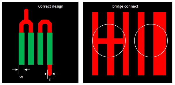
1. Proper Spacing Between Surface-Mount Components
Proper spacing between SMD components is essential for PCB layout. Insufficient spacing may lead to soldering defects like bridging. Refer to the recommended spacing below for better manufacturability.
Spacing for SMD components:
Homogeneous SMD components: ≥0.3mm.
Heterogeneous SMD components: ≥0.13*H+0.3mm (H for maximum height difference of neighboring components).
Spacing for hand-soldering components: ≥1.5mm.

The spacing values provided above serve as a general guideline from WELLER. To ensure manufacturability, always consult with your specific PCB assembly house to align your design with their SMT process capabilities and tolerances.
2. Proper Spacing Between Surface-Mount and Through-Hole Components
As shown below, maintain 1–3 mm spacing between DIP (Through-Hole) and SMD components. Through-hole parts are declining in electronics due to it’s complex soldering and higher cost.


The spacing values provided above serve as a general guideline from WELLER. To ensure manufacturability, always consult with your specific PCB assembly house to align your design with their SMT process capabilities and tolerances.
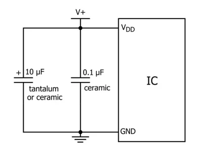
3. Proper Placement of Decoupling Capacitors for ICs
Decoupling capacitors (also known as bypass capacitors) are essential for filtering high-frequency noise in PCB power supply circuits. To optimize circuit performance, each decoupling capacitor should be placed as close as possible to its corresponding integrated circuit (IC) on the PCB layout. If an IC has multiple power supply ports, ensure each port has a dedicated decoupling capacitor for effective noise suppression and stable power delivery.

4. Importance of Component Orientation and Spacing Near the Board Edge
Decoupling capacitors (also known as bypass capacitors) are essential for filtering high-frequency noise in PCB power supply circuits. To optimize circuit performance, each decoupling capacitor should be placed as close as possible to its corresponding integrated circuit (IC) on the PCB layout. If an IC has multiple power supply ports, ensure each port has a dedicated decoupling capacitor for effective noise suppression and stable power delivery.

To ensure a successful panelized design, two critical PCB layout guidelines must be followed:
Guideline 4-1: Orient Components Parallel to the Board Edge
Components near the board border must be placed parallel to the board outline. This orientation allows them to withstand uniform mechanical stress during depanelization. As illustrated in the image above, components placed at an angle (e.g., on the left side) risk being torn from their solder pads due to non-uniform stress, leading to failure.
Guideline 4-2: Maintain a Keep-Out Zone Along the Board Border
A component keep-out zone must be established near the PCB border. This crucial step prevents physical damage to components when the individual boards are separated from the panel, safeguarding your SMT assembly yield.
5. PCB Layout: Optimizing Continuous Pads
For optimal signal timing and integrity, connect a series of SMD pads using serpentine routing rather than direct, straight-line traces. This technique ensures matched trace lengths, which is critical for high-speed signals. Additionally, consistent trace width must be maintained throughout the routing to preserve a controlled impedance.
6. Thermal Management: Heat Dissipation for PADs in Critical PCB Regions
Effective thermal management is a cornerstone of reliable electronics. Without a deliberate PCB layout for thermal dissipation, heat can accumulate in specific areas, leading to performance degradation, component damage, and in extreme cases, a critical fire hazard. Therefore, integrating proactive thermal strategies, particularly through the strategic design of thermal pads, is a fundamental necessity in modern PCB design.


For components with pads over a shared copper region, the routing approach on the right is strongly recommended. The choice between a single trace or multiple traces (e.g., 1 vs. 4) should be determined by the current carrying requirements. The method shown on the left, which floods the pads with a large ground plane, creates significant rework challenges. The copper plane acts as a heat sink, rapidly dissipating thermal energy during desoldering and making component removal exceptionally difficult.
7. PCB Teardrop Design Guidelines for Optimal PCB Layout
Teardrops in PCB layout are specially shaped copper reinforcements applied at the junction of a trace and a pad or via. Their primary function is to provide mechanical and thermal stress relief, preventing hairline cracks at these fragile points. A critical application is at trace width transitions; for instance, when a line narrows from 10 mils to 4 mils, a teardrop at the transition point is essential to distribute stress and enhance manufacturing reliability.


Incorporating teardrops into your PCB layout offers critical benefits for performance, reliability, and manufacturability:
7-1. Enhanced Signal Integrity: Teardrops eliminate sharp, impedance-discontinuities at trace-to-pad junctions. This creates a smoother transition, minimizing signal reflections and preserving integrity, especially in high-speed designs.
7-2. Improved Mechanical Reliability: By reinforcing the high-stress connection between a pad and a trace, teardrops prevent hairline cracks caused by thermal cycling and physical impact during assembly and operation, thereby increasing board longevity.
7-3. Streamlined Manufacturing: The gradual copper taper of a teardrop facilitates a more uniform etch process during PCB manufacturing, preventing acid traps and under-etching issues that can occur at fragile junctions, which improves production yield.
8. Maintaining Consistent Trace Width Between Soldering Pads in PCB Layout
For optimal reliability, the trace width connected to a pad should match the width of the pad’s neck. This practice ensures uniform current distribution and mechanical strength at the connection point.

9. PCB Layout: Leave Unused Pads and Connect to Electrical Ground
All unused IC pins and their pads should be retained and properly terminated by connecting them to the ground plane. Leaving these pins electrically floating can act as miniature antennas, potentially introducing noise into the circuit and compromising overall signal integrity.

10. PCB Layout: Avoid Placing Via Holes on Solder Pads
As a key guideline for DFM, vias should never be placed directly on soldering pads unless absolutely necessary. An open via on a pad will wick solder paste away from the joint during reflow, leading to unreliable, weak connections. The recommended solution is via-in-pad technology, where the via is filled and plated over; however, this advanced process significantly increases fabrication cost and extends lead time.

11. Adequate Spacing Requirements Between Traces/Components and PCB Border in PCB Layout
Maintain a generous keep-out zone between all copper features (traces and components) and the PCB border. This PCB layout guideline is critical for mitigating mechanical stress encountered during panel depanelization, handling, and assembly. The risk is particularly acute for single-layer boards using fragile paper-based substrates (e.g., FR-1), where insufficient clearance can lead to copper cracking and board edge damage.

12. PCB Layout: Electrolytic Capacitor Placement Away from Heat Sources
For reliable performance, always confirm an electrolytic capacitor’s temperature rating and place it away from heat sources in your PCB layout to prevent electrolyte depletion. These basic rules prevent most common assembly issues. For specialized components or complex layout challenges, contact us for expert design assistance to optimize your product’s manufacturability and reliability.

Key Considerations for Electrolytic Capacitor Layout:
Temperature Rating: Ensure the capacitor’s maximum operating temperature rating exceeds the expected thermal environment of your device.
Placement: Position electrolytic capacitors as far as possible from heat-generating components (e.g., power ICs, resistors). Prolonged exposure to heat can cause the internal electrolyte to dry out, leading to premature failure and reduced circuit longevity.
These guidelines provide a solid foundation for a smooth assembly process. However, every project is unique. If you have questions about special components or other PCB layout considerations, we are here to help. Please feel free to contact us for personalized support.


