Home » PCB Fabrication » Via-in-Pad Technology: A Guide to Benefits, Design, and Manufacturing
PCB Fabrication
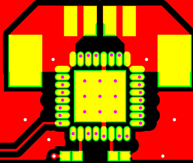
Via In PAD
Also known as a capped via, this technique involves plating over the via hole to create a fully metalized surface. A minimum copper plating thickness of 5μm is required for Class 2, while Class 3 demands 12μm.
Due to the increasingly development of new generation electronics from industry 4.0, 5G technology and AI application, more and more electronics devices are smaller and smaller but working on high speed computing, this requires the base circuit board must be load much more components at smallest size than before. Via in Pad is a solution to the challenge of optimizing the printed circuit board size.
Left: common via design; Right: design with via in pad
CALL US NOW
086 (0755) 2828 2776
Don’t hesitate, contact us to start discussing your projects. We prioritize your inquiries and aim to respond within 12 hours.
What is the Via in Pad in a Printed Circuit Board Layout?
When it comes to PCB layout, or printed circuit board manufacturing, Via in Pad is a special circuit board layout technology to increase PCB density, to allows higher PCB component density (especially in BGA area and SMT IC area). Many electronics engineering designers like to use via in pad technology to significantly save circuit board space so as to load as more components as possible.
PCB layout without via in pad
PCB layout with via in pad
Bottom side review
Top side review
Via in pad PCB assembly
How It Looks Like that Via in Pad in an Existing Printed Circuit Board?
When talk via in pad production process in PCB manufacturing process, it is a process to fill the via holes which locate in the solder PAD by resin (conductive or non-conductive), and then plating copper over these holes and it’s pad and then coating surface finishing. This will make sure the finished PAD without any holes to leak the solder pasting in the PCB assembly process. This technology mostly used in some circuit boards with high precise BGA components assembled, or some PCB board with limited smaller over size and over thickness required.
The best results for you
Quick access to us
Don’t hesitate, contact us to start discussing your projects. We prioritize your inquiries and aim to respond within 12 hours.
Step 1: make the via holes as traditional through via holes.
2
Step 2: filling the via holes by resin(conductive resin or non-conducive resin).
3
Step 3: Plating copper over top side(or both side) of the via holes and it’s Pads, to make sure the via hole to be plated as “shut up”.
4
Step 4: Surface finishing treatment over the Pad.
Via in PAD VS traditional via holes:
The PCB design guidelines on Via-in-pad
Following the design suggestion below or contact us freely when you need to perform a PCB layout on via in pad type.
Via hole size (mm)
0.20
PAD size (mm)
0.40
Annular ring size (mm) per side
0.10
Remark: No matter how big size of your via holes and PAD size is, but the minimum annular ring size must be no less than 0.1mm per side.
For more knowledge about Via in PAD PCB design, you can contact us freely by email: [email protected], our engineer will provide professional consult to your design issues.