PCB LAYOUT & DESIGN

Printed Circuit Board Reverse Engineering

Boost Hybrid PCB reliability and reduce costs with our expert PCB Reverse Engineering Services. We meticulously analyze existing designs to identify optimization opportunities, ensuring robust performance and streamlined manufacturing.

PCB Reverse Engineering Services

PCB Reverse Engineering: When and Why You Need It Most

When facing obsolete electronics with missing design files (Gerber, BOM, schematics, CAD) and unavailable original manufacturers, PCB reverse engineering becomes essential. This process allows you to:

  • Recover lost board designs
  • Recreate accurate schematics
  • Resume production of legacy systems
  • Avoid costly system replacement

With 10+ years of specialized PCB reverse engineering expertise, WELLER Electronics accurately converts physical circuit boards into schematic diagrams and complete documentation.

Recover lost designs, analyze competitors, or modernize legacy systems. We transform physical PCBs into actionable engineering data for reproduction, redesign, or troubleshooting. Request a PCB recovery quote today.

Request a PCB recovery quote today.

Our end-to-end services include:

Schematic Diagram Creating
PCB Design
PCB Layout
BOM Generating
Pick and Place File Generate
Chip Decryption

The best results for you

Quick access to us

Don’t hesitate, contact us to start discussing your projects. We prioritize your inquiries and aim to respond within 12 hours.

PCB to Schematic Reverse and PCB Layout

Absolutely that is an extremely complex and difficult work with requiring great care and experience to convert a PCB to schematic. Our experienced team will do the following work at highly concentrated and skilled manner.
Copy an obsolete printed circuit board (PCB copy).
Re-create lost or missing PCB manufacturing files.
Update an existing populated PCB with new capabilities.
Re-engineer an old PCB design to current standards, compatible to new components.
Re-engineering for cost saving/obsolescence.

Reverse Engineering Process

Only Focusing on 100% Accurate and Proven Process

Facing missing CAD files or obsolete PCB designs? WELLER Technology’s certified reverse engineering process delivers:

Complete PCB Data Recovery:
PCB Reverse Engineering Services
Instead of bearing a long and expensive redesign process, directly ask WELLER Technology to produce the necessary data for your demand. The process of image capture in black and white, gray or color through the conversion of raster to vector data by several quality control steps and finally the output in a wide variety of formats is all work finished in a logical, intuitive and well-designed platform.

Our Streamlined 5-Step Process:

Frequently Asked Questions

About PCBA Reverse Engineering Cost and Work?

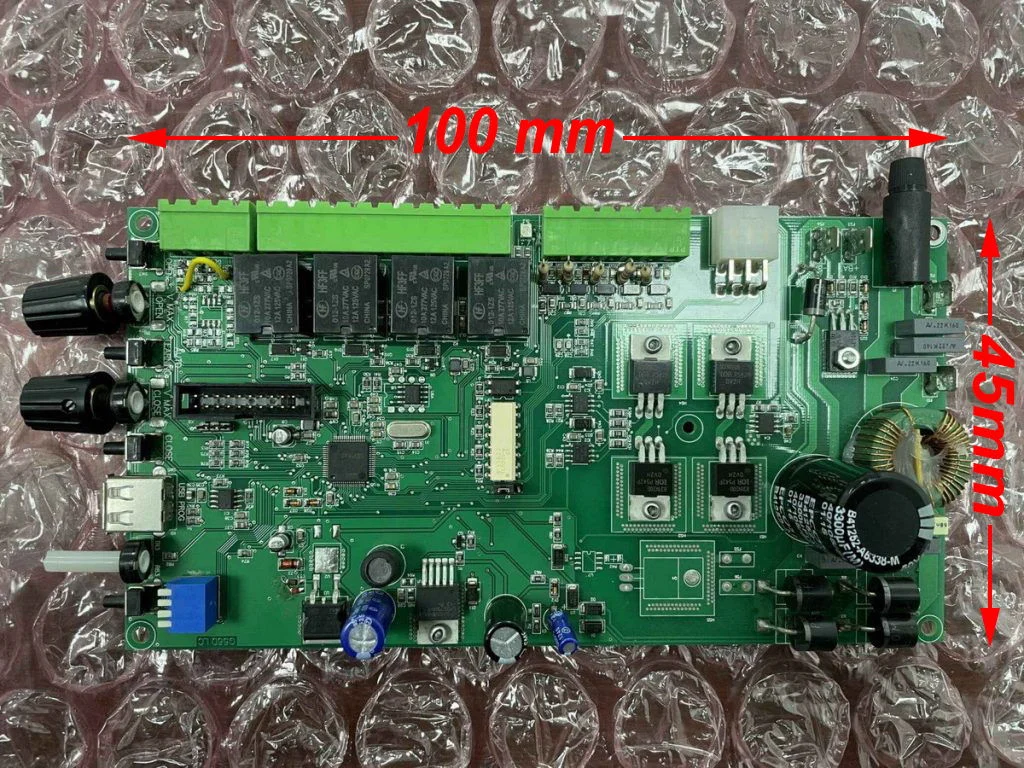
1. In general, it is necessary to provide the exact PCBA picture with viewing from top and bottom side separately, and the size of the circuit board.


How-to-do-PCBA-Reverse-Engineering-Quotation


2. For some special or complex PCBA board, we may need an existing PCBA to have an actual evaluation.

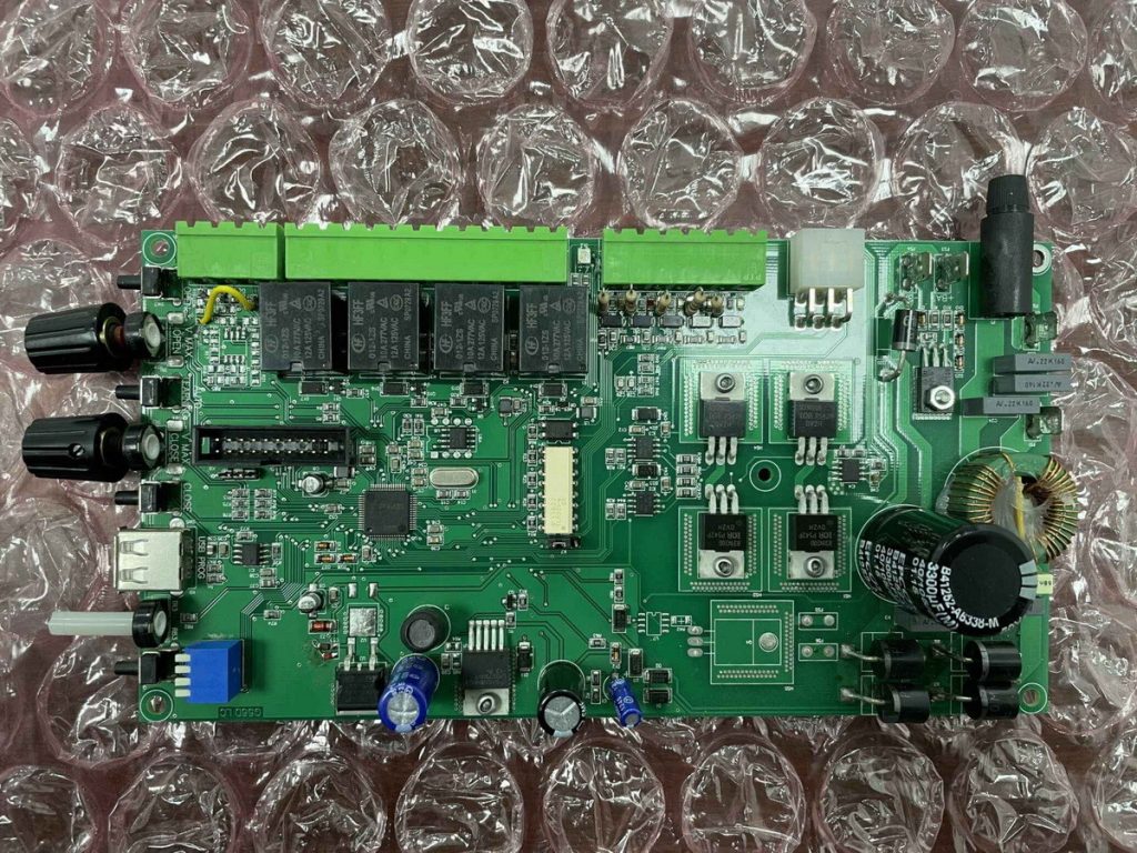
1. 1 pcs PCBA board with fully functionality and stable performance. (The below picture is an example PCBA ready for reversing engineering).


PCB-Reverse-Engineering-top-side-1-1024x768

 
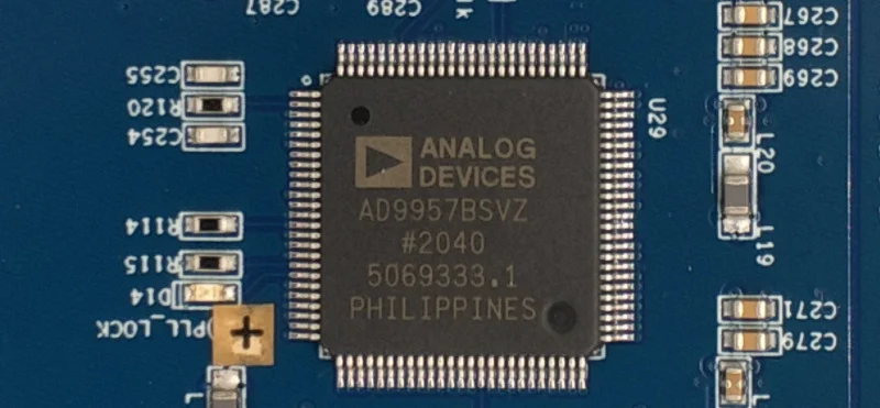
2. In addition to common and generic capacitors and resistors; the silkscreen for some critical complements (such as ICs (chips), diodes and transistors, etc) on the PCBA board should be complete for viewing (the example as shown below for U29).


Components-Silkscreen-guidelines-for-PCBA-Reverse-Engineering-Work