Table of Contents

Eye Diagram Analysis: Fix PCB Signal Integrity Problems

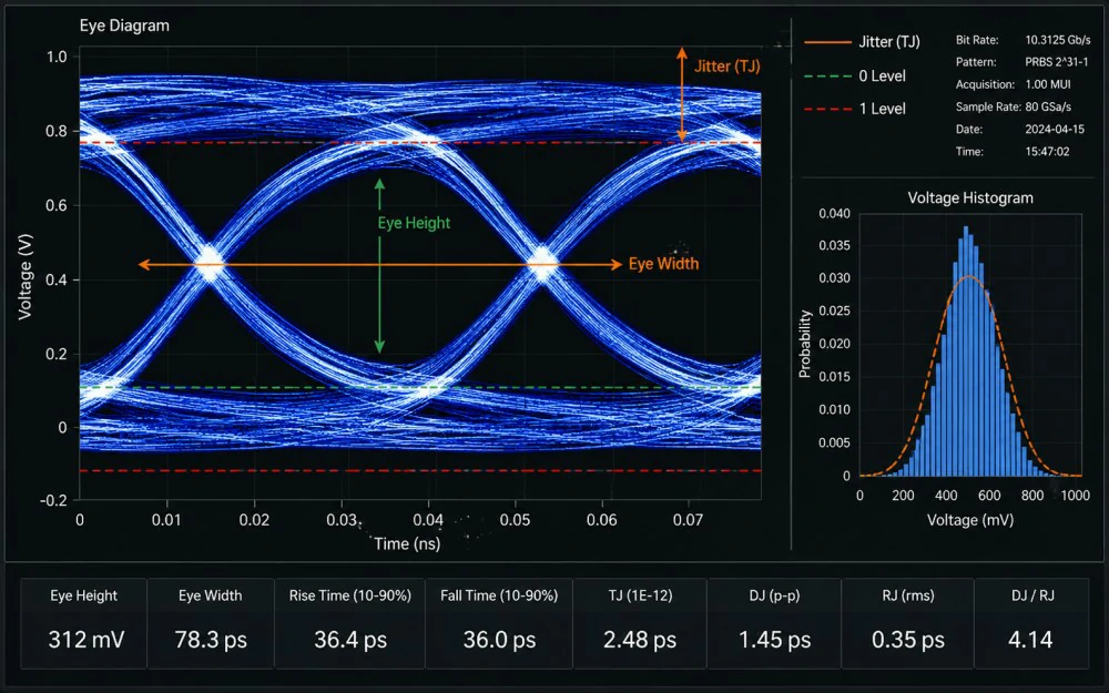
Eye diagram analysis interface showing jitter, eye height, eye width, and voltage distribution
An eye diagram overlays repeated digital transitions to show voltage and timing margin at a selected measurement point. A wide, tall opening usually indicates a cleaner channel. Eye closure can suggest noise, jitter, loss, reflections, crosstalk, skew, or intersymbol interference.
The eye shape does not identify the root cause alone. Engineers must connect the visible symptom to the PCB, components, connectors, transmitter, receiver, or test setup and then confirm it with an appropriate measurement.

What Is an Eye Diagram in PCB?

An eye diagram is a statistical display created by aligning and overlaying many signal transitions within one or more unit intervals. For an NRZ signal, the accumulated traces form an eye-shaped opening between the logic-high and logic-low levels.
Engineers use this display to evaluate sampling margin and identify recurring waveform behavior that may not be visible in a single oscilloscope capture.
  • Eye height represents vertical voltage margin.
  • Eye width represents horizontal timing margin.
  • Crossing position indicates transition symmetry.
  • Waveform spread indicates amplitude noise, timing variation, or both.
  • Mask margin shows separation from a defined exclusion region.

How an Eye Diagram Is Generated

Eye diagram generation process from digital bit stream to overlaid signal transitions
A measured eye is commonly produced with an oscilloscope, a suitable probe or fixture, and a defined data pattern. Waveforms are aligned by a trigger or clock recovery method and folded into repeated unit intervals.
A simulated eye is generated from transmitter, package, PCB, connector, and receiver models. Post-layout analysis may include extracted traces, vias, channel loss, crosstalk, termination, and equalization. Simulation and measurement should use comparable test points and receiver assumptions.

What an Eye Diagram Cannot Prove

An Open Eye Is Not Complete Proof

  • Protocol compliance
  • An acceptable bit error rate
  • Reliable operation across every production condition

Compliance may require a specified data pattern, mask, reference receiver, bandwidth, equalization setting, fixture, and measurement point.

How to Read Eye Diagram Measurements

Annotated NRZ eye diagram showing eye height, width, crossing point, and sampling point
Start with the center opening, then review the crossing region, edge distribution, overshoot, undershoot, and mask margin. No single measurement describes the complete channel.

Eye Diagram Measurement Guide

Technical Table
Eye diagram measurements, their meaning, and possible signal integrity problems
Measurement What It Shows Possible Problem
Eye Height Vertical voltage margin Noise, attenuation, crosstalk, termination error, or power disturbance
Eye Width Horizontal timing margin Jitter, skew, reflections, or intersymbol interference
Crossing Percentage Rising and falling edge symmetry Duty-cycle distortion, threshold error, or unequal slew rates
Rise and Fall Time Signal transition speed Bandwidth limitation, excessive loading, or asymmetric drive
Overshoot and Undershoot Voltage excursions beyond expected logic levels Reflections, poor termination, package resonance, or probing effects
Mask Margin Separation from a defined exclusion region Insufficient compliance margin under the selected test conditions
Interpret each measurement with the interface specification, test point, bandwidth, equalization, and clock recovery method.

Vertical and Horizontal Eye Closure

Vertical closure usually points toward reduced amplitude margin caused by loss, noise, crosstalk, or loading. Horizontal closure more often indicates jitter, skew, reflections, or data-dependent effects. A discontinuity may affect both dimensions, so the visible pattern should be treated as a diagnostic clue rather than proof.

Jitter, BER, NRZ, and PAM4

Eye width becomes more meaningful when it is related to the unit interval and a defined bit error rate.

Unit Interval and Sampling Margin

A unit interval, or UI, is the time allocated to one bit in an NRZ stream. At 10 Gb/s, one UI is 100 ps. If the measured horizontal opening is 58 ps, only 58% of the interval remains visibly open under that test setup. This indicates reduced sampling margin but does not mean total jitter is exactly 42 ps at a specified BER.

Random, Deterministic, and Total Jitter

Random jitter, or RJ, is commonly modeled with Gaussian probability tails. Deterministic jitter, or DJ, includes bounded effects such as duty-cycle distortion, periodic jitter, and data-dependent jitter. Total jitter combines multiple components and must be associated with a specified BER.

BER and Bathtub Curves

A normal eye capture may not include rare errors. A bathtub curve plots estimated error probability against the horizontal sampling position and helps evaluate timing margin at a defined BER. The Tektronix jitter timing fundamentals provide further guidance on jitter decomposition and BER-based analysis.

NRZ and PAM4 Eye Diagrams

NRZ and PAM4 eye diagram comparison with one and three eye openings
NRZ, also called PAM2, uses two voltage levels and creates one main eye opening. PAM4 uses four levels to transmit two bits per symbol and creates three eye openings. Its smaller voltage separation makes it more sensitive to noise, nonlinearity, level mismatch, jitter, and equalization errors.

PCB Causes of Eye Closure

The PCB can introduce attenuation, skew, crosstalk, and reflections through routing geometry, stackup construction, materials, return paths, and layer transitions.

Common PCB Signal Integrity Causes

Comparison of clean, vertically closed, horizontally closed, and distorted eye diagrams
Impedance changes may occur at connectors, component pads, neck-down regions, test pads, layer transitions, and vias. Review controlled-impedance PCB design before changing trace geometry.

Eye Signature Diagnostic Matrix

Evidence Matrix
01

Repeated Edge Distortion

Possible Cause

Impedance discontinuity, via stub, or connector resonance

Confirm With

TDR measurement or extracted channel simulation

Possible Action

Improve transitions, termination, or stub control

02

Reduced Vertical Opening

Possible Cause

Channel loss, noise, crosstalk, or excessive loading

Confirm With

Insertion-loss and aggressor-victim analysis

Possible Action

Shorten routes, increase spacing, or review material loss

03

Horizontal Spreading

Possible Cause

Jitter, differential skew, reflections, or ISI

Confirm With

Timing decomposition and route-length review

Possible Action

Correct skew, return paths, or channel discontinuities

04

Unequal Differential Behavior

Possible Cause

Pair asymmetry, breakout imbalance, or glass-weave interaction

Confirm With

Field-solver analysis or differential measurement

Possible Action

Improve pair symmetry or adjust routing orientation

An eye signature narrows the investigation but does not confirm the root cause until it is supported by measurement or simulation evidence.

Via Stubs and Layer Transitions

Long through-vias can create resonant stubs at high data rates. Review via-stub reflections and back drilling when TDR, simulation, or frequency-domain data identifies a harmful stub.

Stackup and Material Variation

Trace width, spacing, copper thickness, dielectric thickness, and reference-plane distance affect impedance. Insertion loss also depends on dielectric properties, copper roughness, route length, and transition geometry.
Use realistic fabrication data during multilayer stackup planning. A PCB material review can align electrical and manufacturing requirements. Differential pairs may also require attention to glass-weave effects.

PCBA and Component Effects

The bare PCB is only one part of the channel. Packages, connectors, sockets, cables, termination networks, AC-coupling capacitors, protection devices, solder joints, and fixtures can change the final eye.

Component and Interconnect Transitions

Large pads, long leads, unused connector structures, and poorly referenced transitions can add capacitance or inductance. SMT generally supports shorter interconnects, while some through-hole structures create longer stubs. The actual geometry and signal bandwidth determine the risk.

Share critical-net notes, the BOM, pick-and-place files, and assembly drawings during PCB assembly engineering review. DFM changes should preserve the original signal-integrity intent.

Inspection Is Not Signal Validation

AOI can detect visible placement and solder defects, while X-ray can inspect hidden joints such as BGAs. ICT, flying probe, and functional testing address other electrical risks. These methods support quality control but do not replace a defined high-speed channel test.

Simulation and Hardware Validation

High-speed PCB validation workflow from pre-layout analysis to BERT testing
A controlled validation sequence helps separate PCB defects from component, fixture, and receiver effects.

High-Speed Signal Validation Sequence

Process Flow
  1. 1

    Pre-layout Analysis

    Define the stackup, impedance, topology, spacing, and termination targets.

  2. 2

    Post-layout Simulation

    Analyze extracted traces, vias, packages, connectors, loss, and crosstalk.

  3. 3

    PCB Fabrication

    Build the approved stackup with controlled materials and impedance targets.

  4. 4

    TDR and Coupon Verification

    Check impedance consistency and locate significant discontinuities.

  5. 5

    PCBA Measurement

    Measure the assembled channel with the intended fixtures and receiver setup.

  6. 6

    Eye, VNA, and BERT Validation

    Verify timing, loss, reflection, and error performance against acceptance limits.

These methods answer different questions and should be used as a sequence, not treated as interchangeable tests.

Choose the Correct Validation Method

Select the Test by Engineering Question

Decision Guide

What do you need to verify in the high-speed channel?

Eye Diagram

Choose it when: You need to evaluate voltage and timing margin at a selected point.

  • Eye height and eye width
  • Jitter and waveform spread
  • Mask margin and transition quality

Limitation: It does not locate the physical discontinuity by itself.

TDR

Choose it when: You need to find impedance changes along the interconnect.

  • Trace and coupon impedance
  • Via, connector, and transition discontinuities
  • Approximate physical defect location

Limitation: It does not prove complete operating link performance.

VNA

Choose it when: You need frequency-domain channel performance.

  • Insertion loss
  • Return loss and reflections
  • Crosstalk and channel bandwidth

Limitation: Accurate results require suitable fixtures and de-embedding.

BERT

Choose it when: You need to verify actual error performance.

  • Bit error rate under defined conditions
  • Receiver sensitivity and margin
  • Bathtub curves and stress testing

Limitation: A failed BER result may not identify the physical source.

Eye diagrams, TDR, VNA, and BERT provide different evidence. Complex failures often require more than one method before changing the PCB design.

Why Simulation and Hardware May Disagree

Differences may come from inaccurate material data, missing connector or package models, fabrication variation, fixture effects, probe loading, power noise, or receiver settings. Confirm the physical stackup and measurement configuration before changing the layout.

Manufacturing and Test Handoff

High-speed fabrication packages should define the interface, data rate, critical nets, impedance targets, approved stackup, material limits, coupon requirements, and acceptance method.
  • State which trace dimensions the fabricator may adjust.
  • Identify critical vias, connectors, and transition regions.
  • Define responsibilities for simulation, TDR, assembly inspection, and system testing.
  • Record test points, limits, and reporting requirements.
A pre-manufacturing DFM review can resolve build issues before release. Controlled impedance improves consistency but cannot guarantee an open eye because the complete channel includes the transmitter, receiver, packages, connectors, and operating conditions.

Turning Eye Diagram Results into PCB Design Decisions

Treat the eye diagram as a symptom rather than a complete diagnosis. Confirm the measurement setup, separate timing and amplitude effects, and use TDR, VNA, extracted simulation, jitter analysis, or BER testing to verify the suspected mechanism.
The corrective action may involve routing, return paths, vias, termination, materials, components, equalization, or fixtures. Document these decisions so signal-integrity requirements remain consistent through fabrication, assembly, and validation.

Frequently Asked Questions

What does an eye diagram reveal about PCB signal integrity?

It shows voltage and timing margin at a selected point. It can reveal symptoms of noise, jitter, attenuation, reflections, skew, crosstalk, and intersymbol interference, but further testing is normally required to identify the cause.
There is no universal minimum. Acceptable eye height, width, mask margin, and BER depend on the interface specification, data rate, reference receiver, equalization, and required operating margin.
No. Channel performance also depends on loss, vias, packages, connectors, termination, crosstalk, transmitter behavior, receiver settings, fixtures, and fabrication variation.
An eye diagram shows overlaid voltage transitions. A bathtub curve plots estimated error probability against the horizontal sampling position to evaluate timing margin at a defined BER.
The model may omit actual material properties, fabricated geometry, packages, connectors, fixtures, probe loading, power noise, or receiver equalization.
By Kevin

I have over 10 years of experience in PCB manufacturing. My work includes PCB fabrication, SMT assembly, DFM review, supplier communication, and electronics production support. In my writing, I explain PCB design, layer stack-up, assembly processes, quality control, and production planning in a practical way. My goal is to help readers make better manufacturing decisions.

Recent Posts

Get In Touch With Us Today

Drag & Drop Files Here (dsn, pdf, xlsx, dxf, zip, rar up to 8M)
or
This form is protected by Google’s Terms of Service and Privacy Policy.

Related Posts

IPC J-STD-001 requirements for controlled PCB assembly quality and workmanship

IPC J-STD-001 defines material, process, inspection, and acceptance requirements for soldered electrical and.

PCB solder mask materials shown in a cross-section with LPI, dry-film, flexible solder mask, and polyimide coverlay.

PCB solder mask materials are permanent polymer systems applied over copper to protect.

Standardized PCB module design and production risks

Choose flying probe testing for prototypes, changing designs, and high-mix builds. Choose in-circuit.

Leave a Reply

Your email address will not be published. Required fields are marked *