
The glass fiber weave effect, also known as weave skew, is a critical signal integrity challenge in high-speed PCB design that occurs when differential pair traces experience uneven propagation delays due to dielectric constant variations between fiberglass strands and resin. As data rates climb into multi-gigabit ranges (PCIe Gen 5, USB4, 100G Ethernet), even picosecond-level differential pair skew can degrade eye diagrams, increase jitter, and raise bit error rates.
This article explains what the glass fiber weave effect is, why it happens, how it impacts high-speed differential pairs, and proven techniques to minimize weave skew through angled routing, spread glass materials, and advanced laminates.
Understanding PCB Materials
To understand weave skew, it is important to first understand how standard PCB materials are constructed.
Most PCBs are made using FR-4 laminate, which consists of:
- Woven glass fiber cloth
- Epoxy resin
- Copper foil layers

The woven fiberglass provides mechanical strength, while the resin binds the structure together. The problem is that fiberglass and resin have different electrical properties, particularly different dielectric constants.
The dielectric constant (Dk) determines how electromagnetic waves propagate through a material. Since glass fibers have a higher dielectric constant than resin, signals traveling over different portions of the PCB may experience slightly different propagation speeds.
This difference becomes important when routing high-speed differential pairs.

What Is the Glass Fiber Weave Effect?
The glass weave effect occurs when one trace of a differential pair travels primarily over fiberglass strands while the other trace travels over resin-rich regions.
Because the dielectric constants are different:
- One signal travels slightly slower
- The other signal travels slightly faster
This creates a timing mismatch between the two traces, known as skew.
In high-speed systems, even very small timing mismatches can degrade signal quality and increase bit errors.
Why Differential Pairs Are Sensitive to Skew
Differential signaling depends on both signals arriving simultaneously at the receiver. When skew develops:
- The receiver sees a timing imbalance
- Common-mode noise cancellation weakens
- Eye diagrams begin to close
- Jitter increases
- Bit error rates may rise
At lower frequencies, the effect may be negligible. However, modern interfaces operating at several gigabits per second are highly sensitive to even picosecond-level timing mismatches.

- PCIe Gen 5 operates at 32 GT/s
- USB4 supports up to 40 Gbps
- 100G Ethernet uses extremely fast differential signalin
In these systems, weave skew can become a limiting factor for signal integrity.
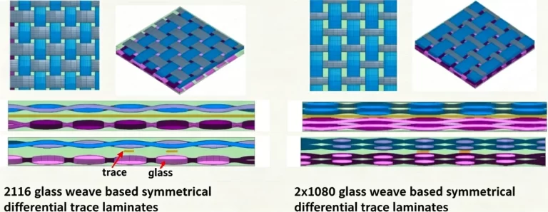
How Fiberglass Weave Is Structured
Fiberglass inside PCB laminates is woven into patterns called weave styles. Common weave styles include:
- 106
- 1080
- 2113
- 2116
- 7628
These numbers describe the density and thickness of the fiberglass weave.
Coarser weaves contain larger glass bundles and wider resin gaps. This increases dielectric variation across the PCB, making weave skew more severe.
Finer weaves distribute fiberglass more evenly, reducing dielectric inconsistencies.
Based Material Line Up S1000H (S1000HB)-PREPREG (B-STAGE)
| Glass style | RC (%) Nominal | Thickness | Dk | Df | |||||||
| mm | mil | 1GHz | 3GHz | 5GHz | 10GHz | 1 GHz | 3 GHz | 5 GHz | 10 GHz | ||
| 7628 | 43* | 0.185 | 7.28 | 4.81 | 4.74 | 4.74 | 4.73 | 0.014 | 0.015 | 0.015 | 0.016 |
| 7628 | 46 | 0.195 | 7.68 | 4.74 | 4.68 | 4.66 | 4.66 | 0.015 | 0.016 | 0.016 | 0.016 |
| 7628 | 48 | 0.205 | 8.07 | 4.70 | 4.63 | 4.61 | 4.61 | 0.015 | 0.016 | 0.016 | 0.017 |
| 7628 | 50 | 0.215 | 8.46 | 4.65 | 4.58 | 4.57 | 4.57 | 0.016 | 0.016 | 0.017 | 0.017 |
| 7628 | 52 | 0.225 | 8.86 | 4.59 | 4.52 | 4.51 | 4.50 | 0.016 | 0.016 | 0.017 | 0.017 |
| 1506 | 48 | 0.160 | 6.30 | 4.70 | 4.63 | 4.61 | 4.61 | 0.015 | 0.016 | 0.016 | 0.017 |
| 1506 | 50 | 0.170 | 6.69 | 4.65 | 4.58 | 4.57 | 4.57 | 0.016 | 0.016 | 0.017 | 0.017 |
| 1506 | 52 | 0.180 | 7.09 | 4.59 | 4.52 | 4.51 | 4.50 | 0.016 | 0.016 | 0.017 | 0.017 |
| 2116 | 52* | 0.113 | 4.45 | 4.59 | 4.52 | 4.51 | 4.50 | 0.016 | 0.016 | 0.017 | 0.017 |
| 2116 | 53* | 0.116 | 4.57 | 4.57 | 4.50 | 4.49 | 4.48 | 0.016 | 0.017 | 0.017 | 0.018 |
| 2116 | 55 | 0.120 | 4.72 | 4.53 | 4.45 | 4.43 | 4.43 | 0.017 | 0.017 | 0.018 | 0.018 |
| 2116 | 58 | 0.130 | 5.12 | 4.45 | 4.38 | 4.36 | 4.36 | 0.017 | 0.018 | 0.018 | 0.018 |
| 3313 | 57 | 0.100 | 3.94 | 4.48 | 4.41 | 4.39 | 4.39 | 0.017 | 0.018 | 0.018 | 0.018 |
| 1080 | 65 | 0.072 | 2.83 | 4.29 | 4.21 | 4.19 | 4.18 | 0.019 | 0.019 | 0.019 | 0.020 |
| 1080 | 68 | 0.081 | 3.19 | 4.21 | 4.13 | 4.11 | 4.11 | 0.020 | 0.019 | 0.020 | 0.020 |
| 1080 | 70 | 0.087 | 3.43 | 4.16 | 4.08 | 4.05 | 4.05 | 0.020 | 0.019 | 0.020 | 0.020 |
| 106 | 73 | 0.050 | 1.97 | 4.09 | 4.01 | 3.97 | 3.97 | 0.020 | 0.020 | 0.020 | 0.020 |
| 106 | 78 | 0.063 | 2.14 | 3.97 | 3.89 | 3.83 | 3.83 | 0.02 | 0.021 | 0.020 | 0.022 |
| Remark: | |||||||||||
| 1) Test by SPDR method. | |||||||||||
| 2) The data above show actual values and are not guaranteed, for your reference only. | |||||||||||
| 3) RC* is not common type for reference. | |||||||||||
| 4) Last update: Oct, 2025 | |||||||||||
How the Glass Fiber Weave Effect Causes Skew
Imagine two traces in a differential pair routed side by side:
- One trace may align directly over a glass bundle
- The other may align with resi
Since glass has a higher dielectric constant, the signal above the glass travels more slowly.
Over a long routing distance, the accumulated timing difference becomes measurable.
Example Scenario
Suppose one trace propagates at a slightly lower velocity. Understandably, the other travels faster. If the differential pair length is several inches long, it may result in several picoseconds of skew, enough to distort signals at high data rates.
This effect becomes worse when:
- Differential pairs are long
- Data rates are extremely high
- Coarse glass weaves are used
- Traces align parallel to weave patterns
Suggested Reading: 5G PCB Design Guide: High-Frequency Materials & Tips
Symptoms of the Glass Fiber Weave Effect on Eye Diagrams
Weave skew may produce several signal integrity problems.
Common Symptoms
- Increased jitter
- Reduced eye opening
- Higher bit error rate (BER)
- Differential-to-common-mode conversion
- Timing margin reduction
- Receiver synchronization issues
These issues are often difficult to diagnose because the PCB may appear electrically correct during standard design checks.
Eye Diagram Impact
An eye diagram visually represents signal quality in high-speed systems. When weave skew increases:
- The eye opening becomes smaller
- Timing uncertainty increases
- Signal transitions become less predictable
A closed eye diagram indicates that the receiver has difficulty distinguishing between logic states.
This directly affects communication reliability.

Which Interfaces Are Most Affected?
Some interfaces are particularly sensitive to weave skew because of their very high operating speeds.
Commonly Affected Interfaces
- PCIe
- USB 3.x and USB4
- HDMI
- DisplayPort
- SATA
- DDR memory interfaces
- Ethernet backplanes
- SerDes channels
As signaling speeds continue increasing, weave skew has become an important design consideration across many industries.
5 Methods to Reduce the Glass Fiber Weave Effect
Engineers use several routing and material strategies to reduce weave skew.
1. Routing Differential Pairs at an Angle
One of the most common solutions is routing differential pairs at a slight angle relative to the glass weave pattern.
Instead of routing traces perfectly horizontal or vertical, designers use:
- 10°
- 15°
- Small zig-zag patterns
This ensures both traces experience an average mix of glass and resin over the routing path.
Advantages
- Simple implementation
- No special materials required
- Effective for many designs
Limitations
- Increases routing complexity
- May consume additional PCB area
2. Using Spread Glass Materials
Modern PCB manufacturers offer spread glass laminates, where fiberglass strands are flattened and distributed more evenly.
Benefits include:
- Reduced resin gaps
- More uniform dielectric constant
- Lower differential skew
Spread glass materials are widely used in high-speed networking and server applications.

3. Reducing Differential Pair Length
Shorter traces accumulate less skew over distance. So, designers try to:
- Place components closer together
- Minimize unnecessary routing length
- Avoid long serpentine compensation section
This reduces overall propagation mismatch.
4. Tight Differential Pair Coupling
Closely spaced differential traces experience more similar dielectric environments. It helps with
- Improved noise immunity
- Reduced skew sensitivity
- Better signal consistencys
However, spacing must still satisfy impedance requirements.
5. Choosing Better PCB Materials
Some high-speed laminates are specifically designed for low skew applications.
Examples include:
- Megtron series
- Tachyon materials
- Isola high-speed laminates
- Rogers materials
These materials provide:
- Lower dielectric variation
- Better high-frequency performance
- Reduced insertion loss
Such materials are common in data centers, telecom equipment, and RF systems.
Comparison of Mitigation Techniques
Technique
Cost Impact
Effectiveness
Complexity
Common Usage
Angled Routing
Low
Good
Moderate
General high-speed PCBs
Spread Glass
Medium
Excellent
Low
Servers and networking
Shorter Routing
Low
Moderate
Moderate
Compact PCB designs
Tight Pair Coupling
Low
Moderate
Moderate
High-speed digital systems
Advanced Materials
High
Excellent
Low
Aerospace and telecom
Simulation and Analysis
Modern signal integrity tools can predict weave skew before manufacturing.
Common simulation tools include:
- Cadence Sigrity
- Ansys HFSS
- Keysight ADS
- HyperLynx
These tools help engineers analyze:
- Differential skew
- Propagation delayEye diagrams
- Impedance variation
- Electromagnetic coupling
Simulation has become essential for designs operating above several gigabits per second.
Suggested Reading: PCB Design Tools Guide 2026: Boost Development
Manufacturing Considerations
PCB manufacturers also play a role in reducing weave skew.
Important manufacturing considerations include:
- Selecting proper laminate styles
- Maintaining consistent layer alignment
- Using controlled dielectric materials
- Following impedance control requirements
Communication between PCB designers and fabricators is extremely important for high-speed projects.
Is Weave Skew Always a Problem?
For lower-speed systems, weave skew may have little practical impact. Many consumer electronics function normally despite minor skew effects.
The problem becomes serious when:
- Data rates are extremely high
- Timing margins are very small
- Trace lengths are long
- Signal integrity requirements are strict
As a general rule, the higher the signaling speed, the more important weave skew becomes.
Future Trends in Managing the Glass Fiber Weave Effect
The demand for faster digital communication continues to grow rapidly. Emerging technologies such as:
- AI accelerators
- 800G Ethernet
- High-speed backplanes
- Advanced automotive systems
- Data center networking
are pushing PCB materials and routing methods to their limits.
Future trends include:
- Wider adoption of spread glass laminates
- Improved low-loss dielectric materials
- Better simulation techniques
- AI-assisted signal integrity optimization
- Increased use of advanced packaging technologies
As operating frequencies continue increasing, controlling weave skew will become even more important.
Conclusion
Glass fiber weave effect, or weave skew, is an important signal integrity challenge in modern high-speed PCB design. The problem arises because woven fiberglass and resin have different dielectric properties, causing unequal propagation delays in differential pairs.
While the effect may be negligible at lower speeds, modern multi-gigabit interfaces are highly sensitive to timing mismatches. Excessive skew can increase jitter, reduce eye openings, and degrade overall communication reliability.
Fortunately, engineers have several effective mitigation strategies available, including angled routing, spread glass materials, improved PCB laminates, tighter differential pair coupling, and careful layout optimization.
As digital systems continue moving toward higher data rates, understanding weave skew is becoming an essential skill for PCB designers and signal integrity engineers alike.


