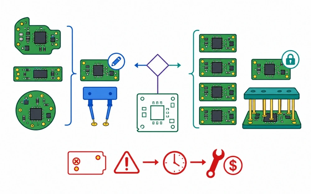
Choose flying probe testing for prototypes, changing designs, and high-mix builds. Choose in-circuit testing (ICT) when the PCB and BOM are stable and recurring volume can justify a custom fixture.
Make this decision before layout release. Missing test access can reduce coverage, extend programming time, and increase fixture or redesign costs.
In Circuit Test vs Flying Probe: Which Method Fits Your PCBA?
ICT uses a fixed bed-of-nails fixture. Flying probe uses programmable moving probes. This interface difference affects tooling cost, cycle time, revision flexibility, and fault diagnosis.
| Decision Factor | In-Circuit Testing | Flying Probe Testing |
|---|---|---|
| Test interface | Custom fixed fixture | Programmable moving probes |
| Initial cost | Higher fixture and program NRE | Lower tooling cost |
| Cycle time | Usually faster after validation | Usually slower due to probe movement |
| Design changes | May require fixture rework and revalidation | Often handled through program updates |
| Opens and shorts | Strong coverage with planned access | Suitable for accessible nets |
| Component measurements | Fast for programmed components | Flexible but slower |
| Hidden solder joints | Cannot directly inspect every joint | Cannot directly inspect every joint |
| Typical fit | Stable recurring production | Prototype, NPI, and high-mix production |
How ICT Uses a Fixed Fixture

ICT contacts planned targets through a board-specific fixture. Depending on the equipment and program, it can detect opens, shorts, missing parts, wrong values, polarity faults, and selected device failures. See how in-circuit testing supports PCB quality.
Because the fixture follows the physical layout, an engineering change may require new pins, wiring changes, program updates, or fixture replacement.
How Flying Probe Reduces Dedicated Tooling

A flying probe tester moves between accessible pads, vias, leads, and connector pins. Programs are commonly developed from the schematic, BOM, and net-aware manufacturing data. WellerPCB’s guide to flying probe testing for PCB evaluation explains the process.
It remains limited by target access, probe clearance, travel distance, measurement count, and machine configuration.
Practical Selection Rule
Use flying probe while the layout, BOM, or firmware interface may change. Consider ICT after design freeze when repeated orders and shorter cycle time can offset fixture investment.
Design and Assembly Factors That Affect Testability
Neither method can compensate for poor access. Testability depends on layout, package selection, component height, panel format, and board support.
Separate DFM, DFA, and DFT
DFM checks fabrication risks. DFA checks placement and soldering risks. DFT checks test targets, probe clearance, support, isolation, and electrical coverage. An early DFM review before PCB manufacturing can identify layout conflicts, but it does not replace a dedicated DFT review.
Confirm Reachable Test Targets

Possible targets include dedicated test pads, exposed through-vias, through-hole leads, connector pins, and accessible component pads. Blind vias, buried vias, covered microvias, and targets under components may be inaccessible.
Request equipment-specific limits for target size, probe pitch, component clearance, board dimensions, warpage, and one- or two-sided access. These limits vary by machine and supplier.
Check Package and Mechanical Constraints
BGA, QFN, CSP, and other bottom-terminated packages block direct contact with hidden joints. ICT or flying probe may test connected nets elsewhere, but X-ray or boundary scan may still be required.
Tall connectors, shields, heatsinks, and dense double-sided placement can obstruct probes or fixture hardware. Board support must also control flex under probe force.
Review Panelization and Contact Surfaces
Decide whether testing occurs in-panel or after depanelization. Rails, tooling holes, fiducials, breakout tabs, and component overhang affect loading and fixture design.
ENIG, HASL, and OSP do not select the method by themselves. Contact reliability also depends on oxidation, residue, solder-mask clearance, and repeated probing.
Avoid Common Testability Mistakes
Most access problems are easier to correct during layout than after test development begins.
- Do not wait until production release to review test access.
- Do not assume every via is a suitable probe target.
- Keep tall parts and shields away from planned access points.
- Provide practical power and ground access.
- Update test data after every approved engineering change.

Cost, Lead Time, and Product Lifecycle
Compare total lifetime cost rather than fixture price alone. Include programming, handling, cycle time, maintenance, retest, storage, and engineering changes
| Cost Input | ICT | Flying Probe |
|---|---|---|
| Initial engineering | Fixture, program, and validation | Program and validation |
| Per-board cost | Often lower at stable volume | Often higher due to longer test time |
| Revision cost | Fixture and program may change | Program changes are usually easier |
| Maintenance | Pins, wiring, alignment, and storage | Probe condition and program control |
Calculate the Economic Crossover

Use this model only when both methods meet the required coverage and flying probe has a higher variable cost per board:
Break-even quantity = (ICT NRE – flying-probe setup cost) / (flying-probe cost per board – ICT cost per board)
Example: ICT requires $5,000 in fixture and programming cost, flying probe requires $500 in setup, and ICT saves $9 per board. The estimated crossover is 500 boards. These figures are illustrative; actual quotations must include handling, debug, maintenance, retest, and expected revisions
When to Move from Flying Probe to ICT
A product can start on flying probe during NPI and move to ICT when:
- The PCB layout and controlled BOM are frozen.
- Recurring order volume is predictable.
- Flying-probe cycle time limits throughput.
- Per-board savings can recover fixture NRE.
- Engineering change frequency has fallen.
High-mix production may remain on flying probe even when total factory volume is high because each assembly has limited stable demand. See WellerPCB’s guidance on prototype-to-production NPI planning.
Coverage and Supporting Inspection Methods
ICT and flying probe provide electrical evidence, but neither method replaces inspection or powered functional verification.
Define Coverage Before Comparing Quotes
- Net coverage: the accessible connections checked for opens or shorts.
- Component coverage: the parts that can be measured or verified.
- Fault coverage: the defect types the program is designed to detect.
- Functional coverage: the powered behaviors confirmed by the test plan.
Ask each supplier to list inaccessible nets, excluded components, planned measurements, and reporting methods. WellerPCB’s overview of integrated testing for PCB reliability explains why multiple methods may be necessary.
Combine Electrical Test with Other Evidence
| Method | Primary Role | Key Limitation |
|---|---|---|
| SPI | Checks solder-paste deposition | Occurs before component placement |
| AOI | Checks visible placement and solder features | Cannot fully inspect hidden joints |
| AXI | Examines hidden solder structures | Does not prove electrical function |
| Boundary scan | Tests supported digital interconnects | Requires compatible devices and design support |
| Functional test | Checks powered product behavior | May provide less precise fault isolation |
Use AOI for PCB assembly for visible defects, X-ray for hidden solder structures, and IEEE 1149.1 boundary scan where supported. Add firmware programming and functional testing when the product must be verified under power.
Supplier Data and Responsibility

Complete, revision-controlled inputs reduce quotation errors and program delays.
Provide a Controlled Test Package
- Controlled BOM and approved substitutions
- Schematic and relevant component datasheets
- ODB++, IPC-2581, or other net-aware data
- Gerber, pick-and-place, and assembly drawings
- Test limits, firmware, and revision history
Gerber files show geometry but may not contain enough connectivity or component data for complete test development.
Use Standards Within Their Scope
IPC-A-610 acceptance criteria and J-STD-001 soldering requirements can support a PCBA quality specification, but they do not define complete ICT or flying-probe coverage. State the required acceptance class and customer-specific requirements in the RFQ.

Clarify Commercial and Quality Ownership
For ICT, confirm who owns, stores, maintains, repairs, and updates the fixture. For both methods, define test records, failure codes, retest policy, revision control, serial-number traceability, and revalidation after component substitutions.
Review the supplier’s PCB assembly capabilities against the required test access, inspection plan, and reporting format.
Choosing the Right PCBA Test Strategy
Flying probe is usually the safer choice while a design is changing. ICT becomes more attractive when the assembly is stable, access is planned, and recurring volume can recover fixture cost. Final selection should be based on required coverage, verified DFT access, lifetime cost, and the supporting AOI, X-ray, boundary-scan, or functional-test plan.
For a product moving from prototype to recurring production, discuss the NPI and PCBA test strategy before finalizing test pads and fixture requirements.
Frequently Asked Questions
When Does an ICT Fixture Become Economical?
There is no universal quantity. Compare fixture and programming NRE with per-board test savings, expected lifetime volume, revision risk, maintenance, handling, and retest costs.
Can Flying Probe Work Without Dedicated Test Pads?
Sometimes. It may contact accessible vias, leads, connector pins, or component pads. The targets must still meet the tester’s size, clearance, and contact requirements.
Can One PCBA Use Both Flying Probe and ICT?
Yes. Flying probe may support prototypes and early NPI builds, while ICT is introduced after design freeze for stable recurring production.
Can ICT or Flying Probe Test BGA and QFN Connections?
They can test connected nets through accessible points, but they cannot directly inspect every hidden solder joint. X-ray or boundary scan may be needed.
Which Files Does a Testing Supplier Need?
Typical inputs include a controlled BOM, schematic, net-aware manufacturing data, Gerber files, pick-and-place data, assembly drawings, test limits, firmware, and revision history.
Post Views: 24